Lab 02 - EE 421L
----------------------------------------------------------------------------------------------------
Pre-lab:
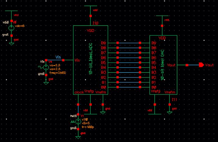
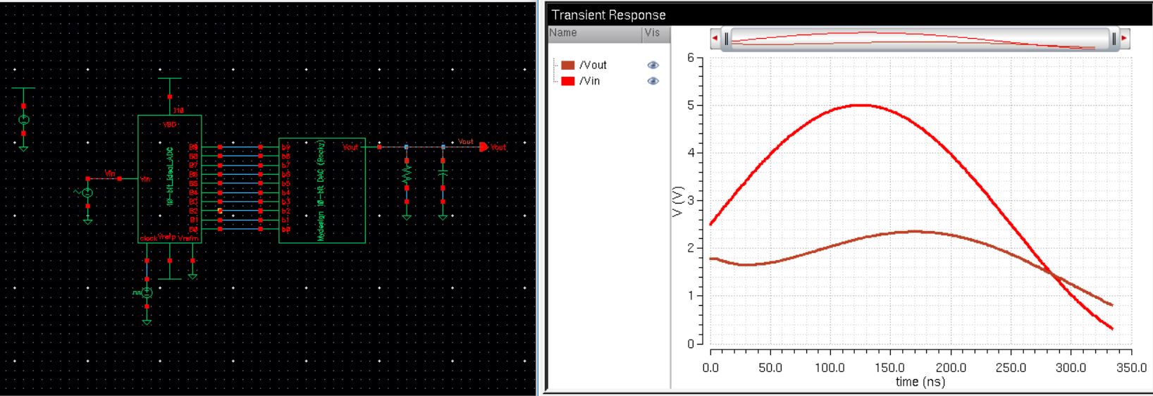
Prior to starting the design for a 10-bit DAC, we've installed the schematic into Cadence to gain a better understanding of a DAC.
-> The file lab2.zip is downloaded, and uploaded to the Unix server (in the CMOSedu directory).
-> The file is extracted using the "unzip lab2.zip" statement.
-> Then opening the "cds.lib file", the statement "DEFINE lab2 $HOME/CMOSedu/lab2" is added to the file.
We can then open the schematic through the Cadence library under the "lab2" folder.
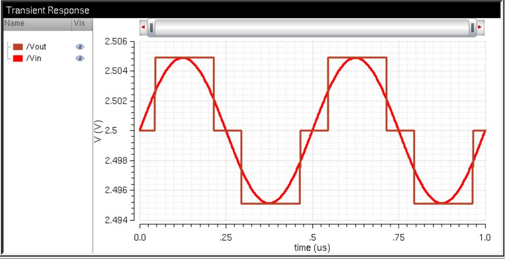
By observing the DAC, we can increase the voltage pulse and examine that the system clips due to surpassing the the voltage supplied from the reference voltages.
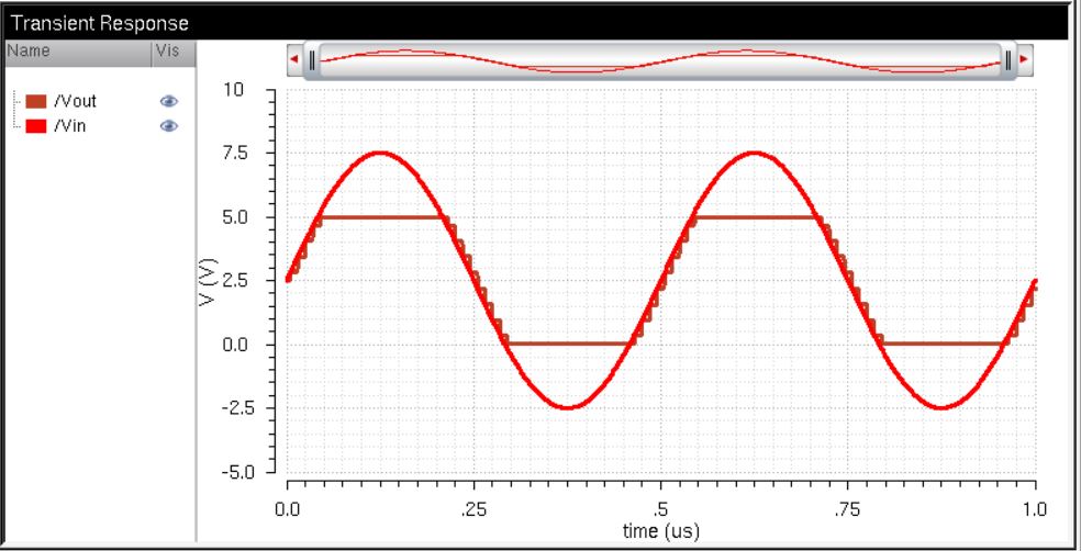
The 10-bit DAC therefore somehow breaks the total voltage into 10 components representing different bits of the signal.
Mathamatically, this will follow:
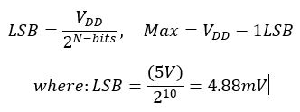
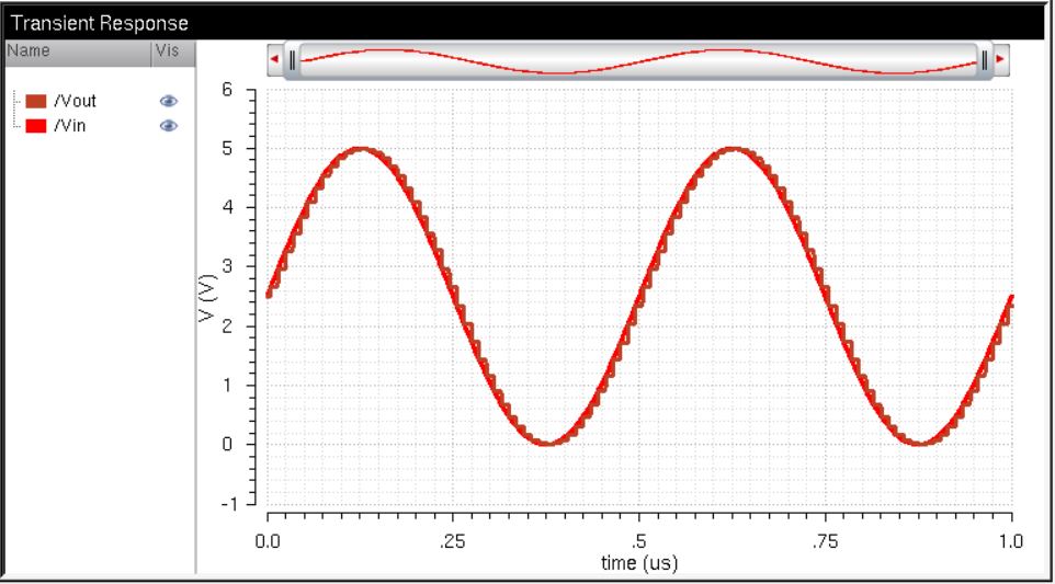
By representing the voltage input as 1 LSB, we can see that the voltage sinusoidal is represented as a one bit signal (0000 0001).
 .
.
----------------------------------------------------------------------------------------------------
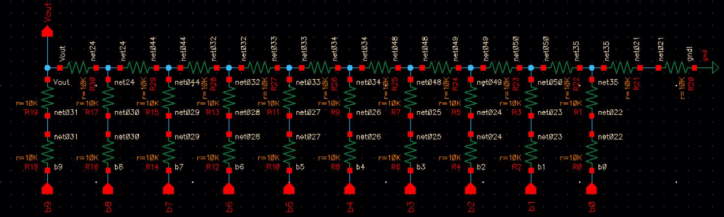
Step 1: Design a 10-bit DAC using an n-well R of 10k:
Step 2: Determine Output Resistance of the DAC. Recall:
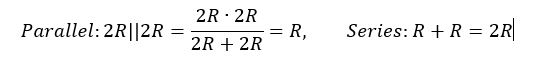
By combining the resistors (from ground towards Vout), we can observe the Load Output resitance will become 1 R (10k).
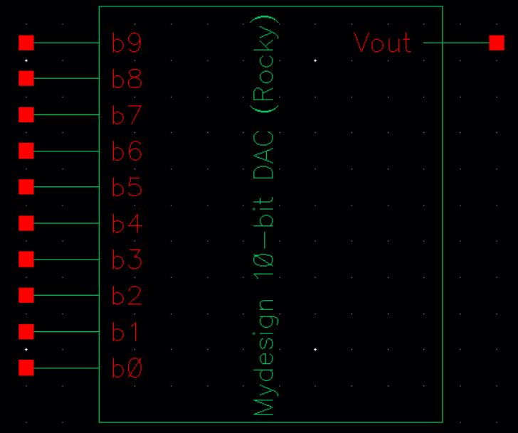
Using the previous DAC schematic, we can create a symbol by clicking Create->Cellview->From Cellview.This symbol can then be used to create new schematics.
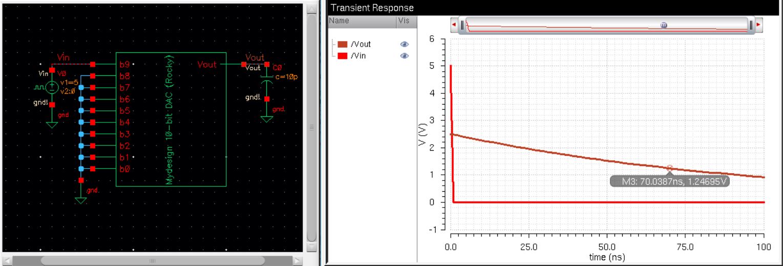
Step 3: Observe delay by driving a load.
-> Ground all input terminals of the DAC except for input B9,
-> Connect B9 to a pulse source (0V-Vdd). Let "Vdd = 5V".
-> Connect a 10pF Load.
Check: 0.7RC = 0.7(10k)(10pF) = 70ns, where: 50% of 2.5V -> 1.25V as shown below.
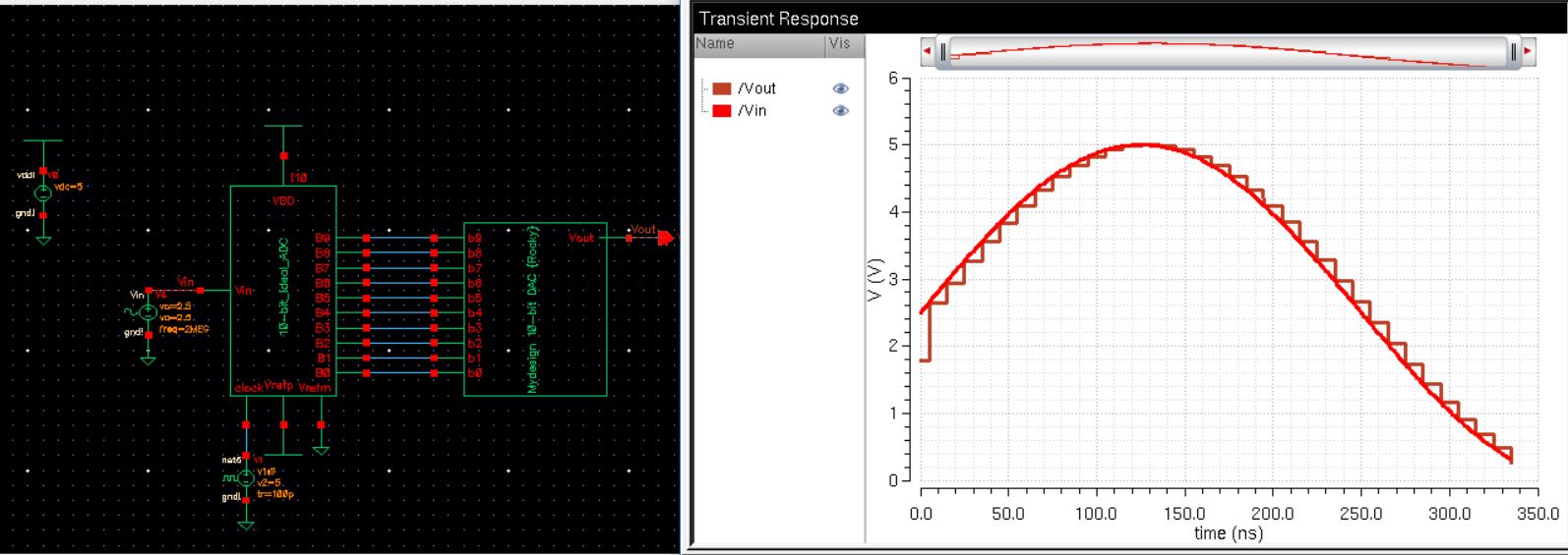
Step 4: Verify the DAC works properly.
By copying the sim_Ideal_ADC_DAC as a new schematic, we can replace the original DAC symbol for the newly made one.
By simulating the schematic, we would then produce the same results as the original DAC.
----------------------------------------------------------------------------------------------------
Simulations:
Driving a 10k Load resistance:
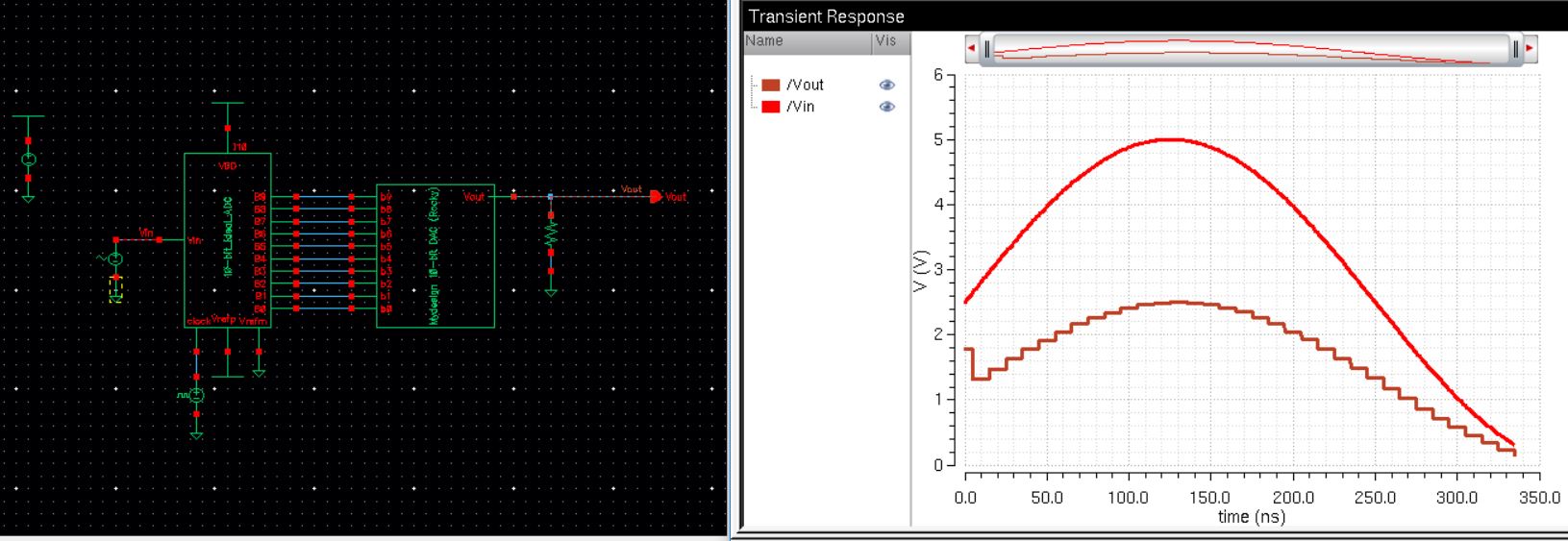
Driving a 10pF capacitance:
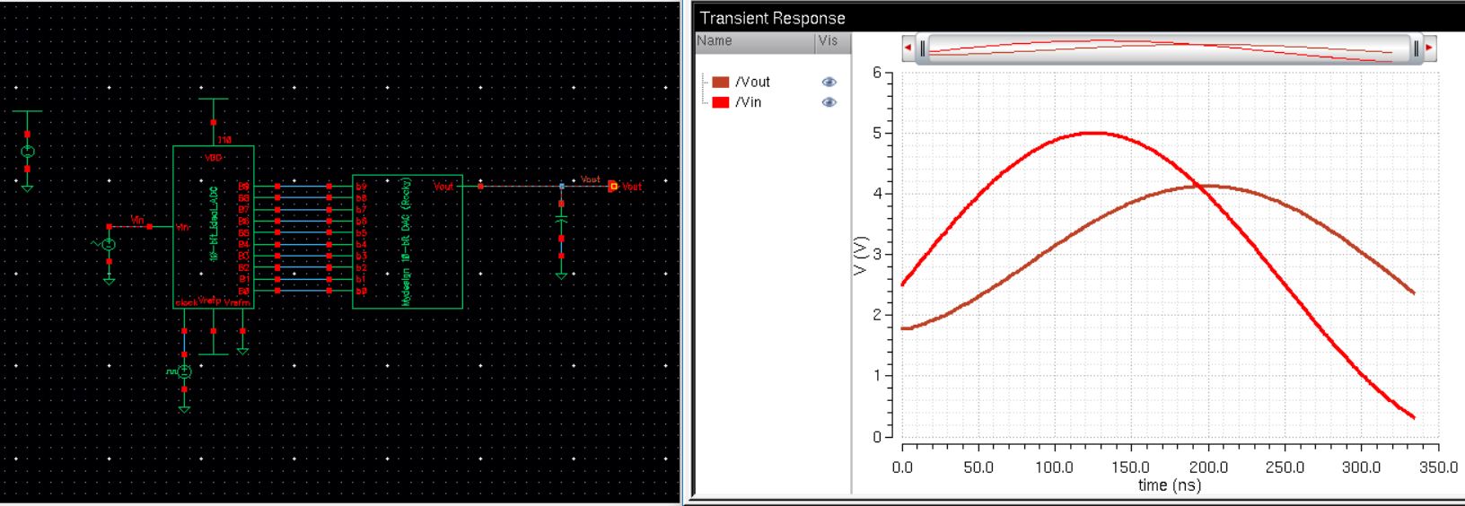
Driving an RC Load (10k resistance, 10pF resistance):
Since the ouput load of the DAC is already 10k resitance, adding a new 10k load to the entire circuit creates a voltage divider.
This output voltage is thus half of the output voltage without added load.
----------------------------------------------------------------------------------------------------
The labs are backed up through a saved directory in my computer as well as into my google drive account:
This Concludes the Lab 2 Report.