Lab 7 - EE 421L
Authored
by Biruk Gebremeskel
Email: gebreb1@unlv.nevada.edu
Novemeber 7, 2018
Lab
description:
The
purpose of this lab was to help us get use to using buses and arrays in
the design of word inverters, muxes, and high speed adders.
Pre-Lab Work:
All previous labs have been backed up in Dropbox
Lab Work:
Exercise 1
4Bit Word Inverter
Schematic
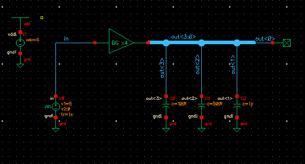 | Simulation
|
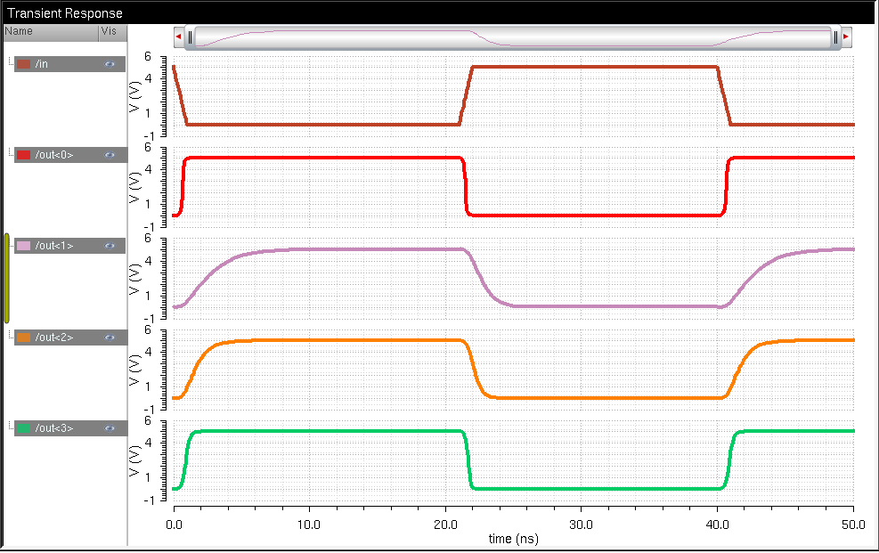
From the above simulations we can see that the delay increased as the capactive load increasesd.
Exercise 2
8 Bit input /output array of AND, OR, NOR, and NAND, and Inverter gates
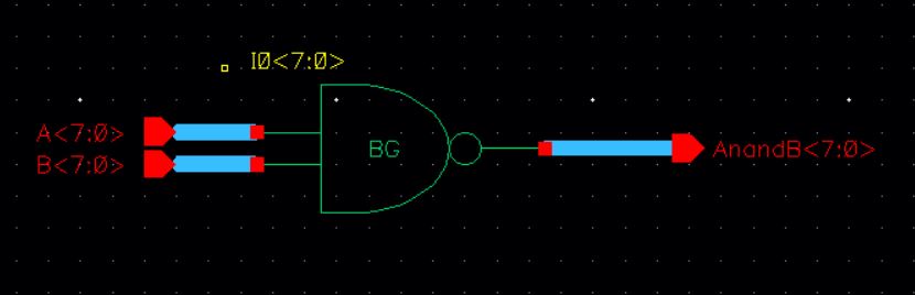
8-Bit NAND gate Schematic
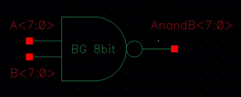
| 8-Bit NAND gate Symbol
|
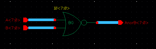
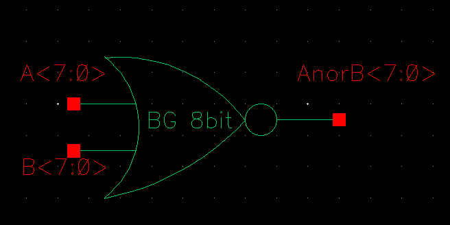
8-Bit NOR gate Schematic
 | 8-Bit NOR gate Symbol
 |
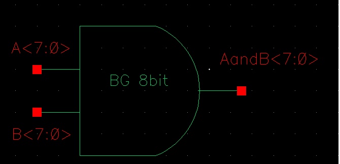
8-Bit AND gate Schematic
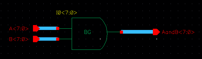 | 8-Bit AND gate Symbol
|
8-Bit OR gate Schematic
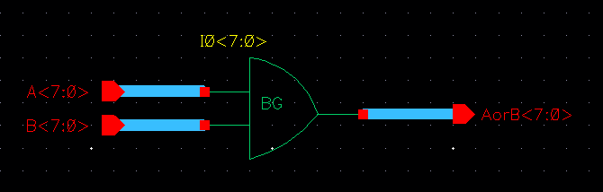 | 8-Bit OR gate Symbol
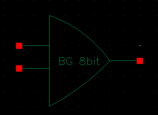 |
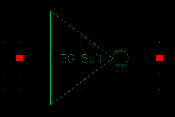
8-Bit Inverter Schematic
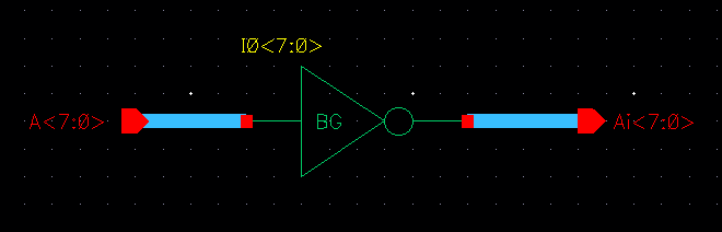 | 8-Bit Inverter Symbol
 |
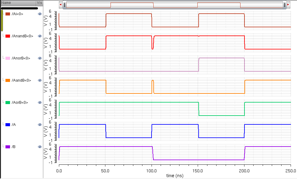
8-Bit Logic gate Schematic
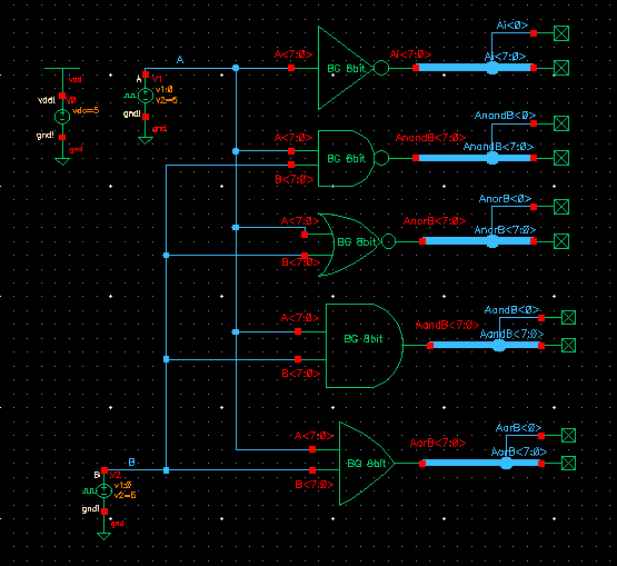
8-Bit Logic gate Simulation
Exercise 3
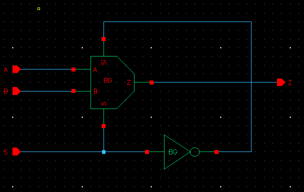
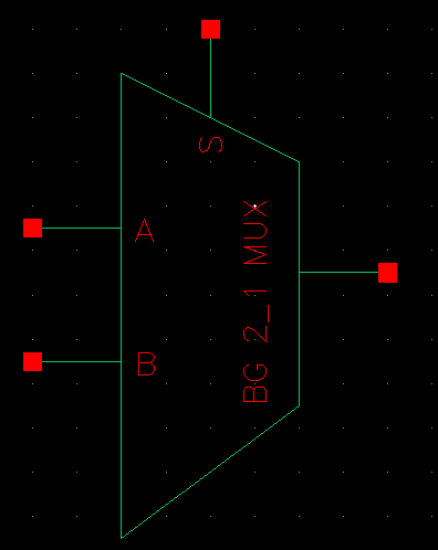
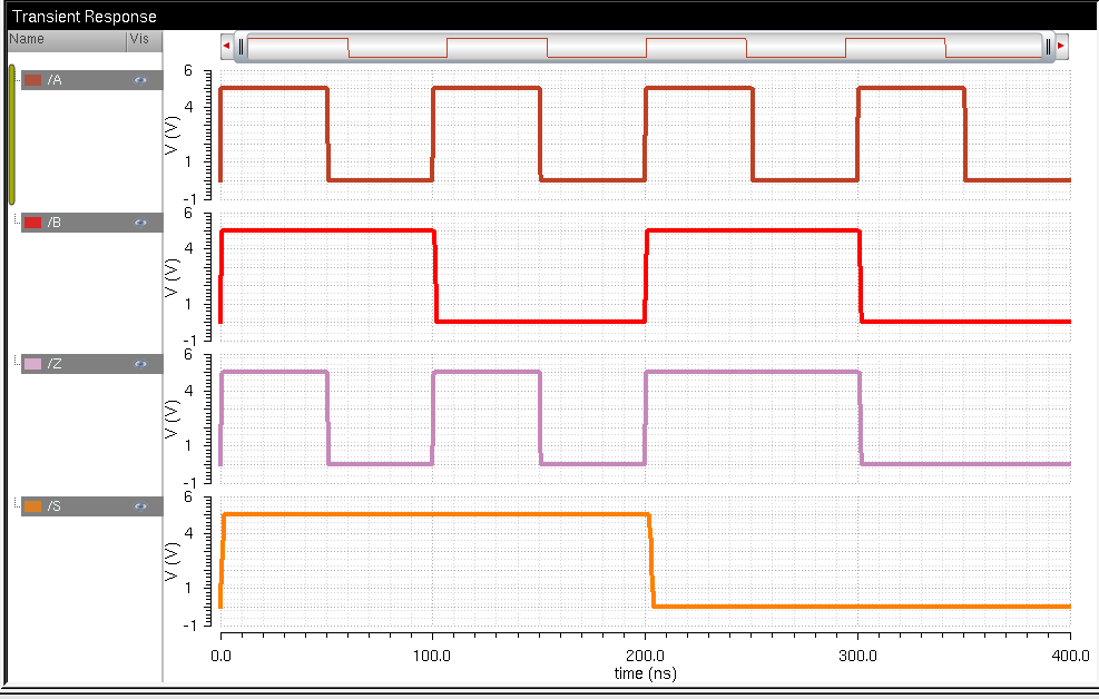
2-1 MUX/DEMUX Schematic, Symbol, and Simulation
Exercise 4
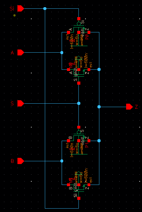
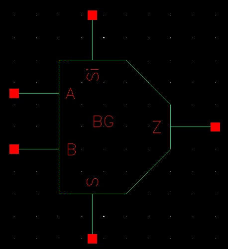
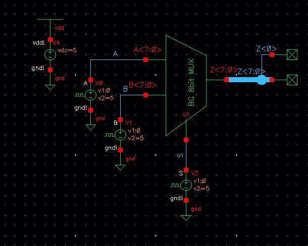
2-1 MUX/DEMUX Schematic and symbol with a single select
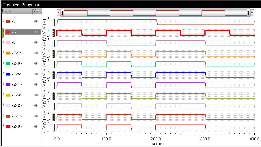
8-Bit 2-1 MUX/DEMUX Schematic, and Simulation
EXercise 5
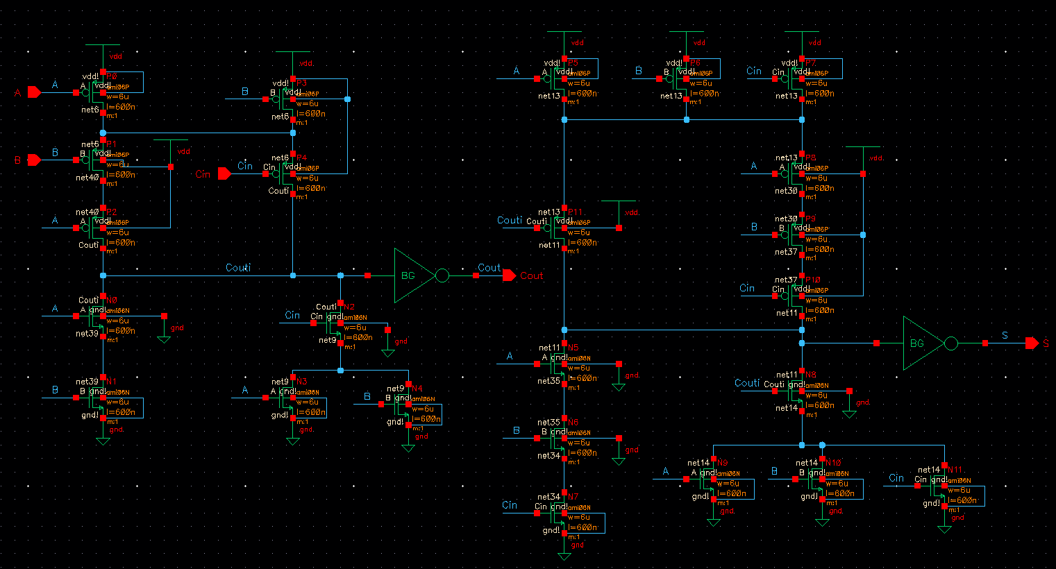
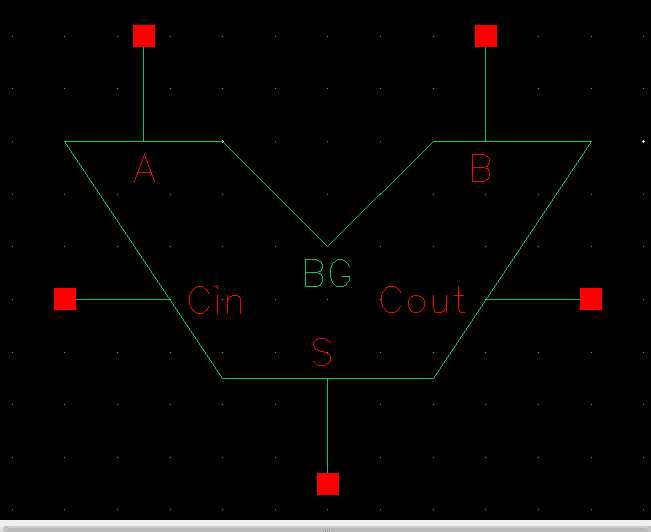
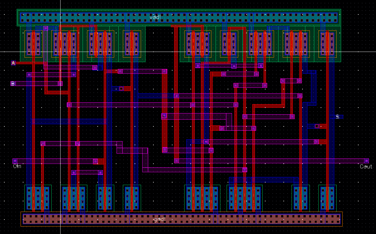
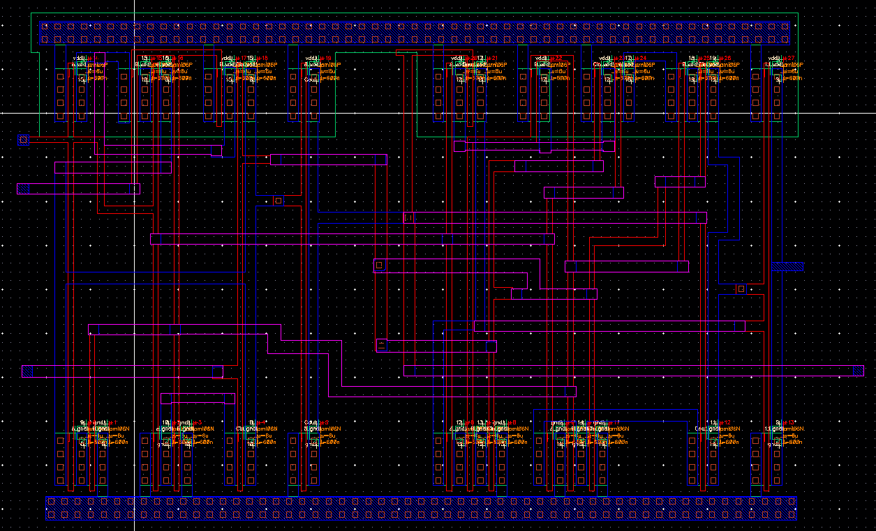
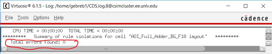
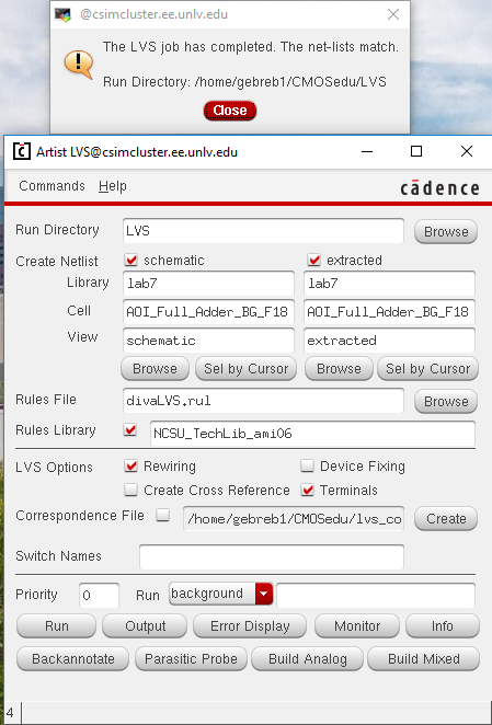
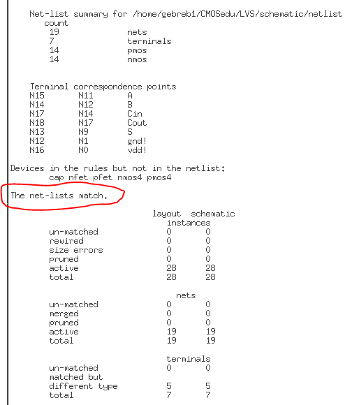
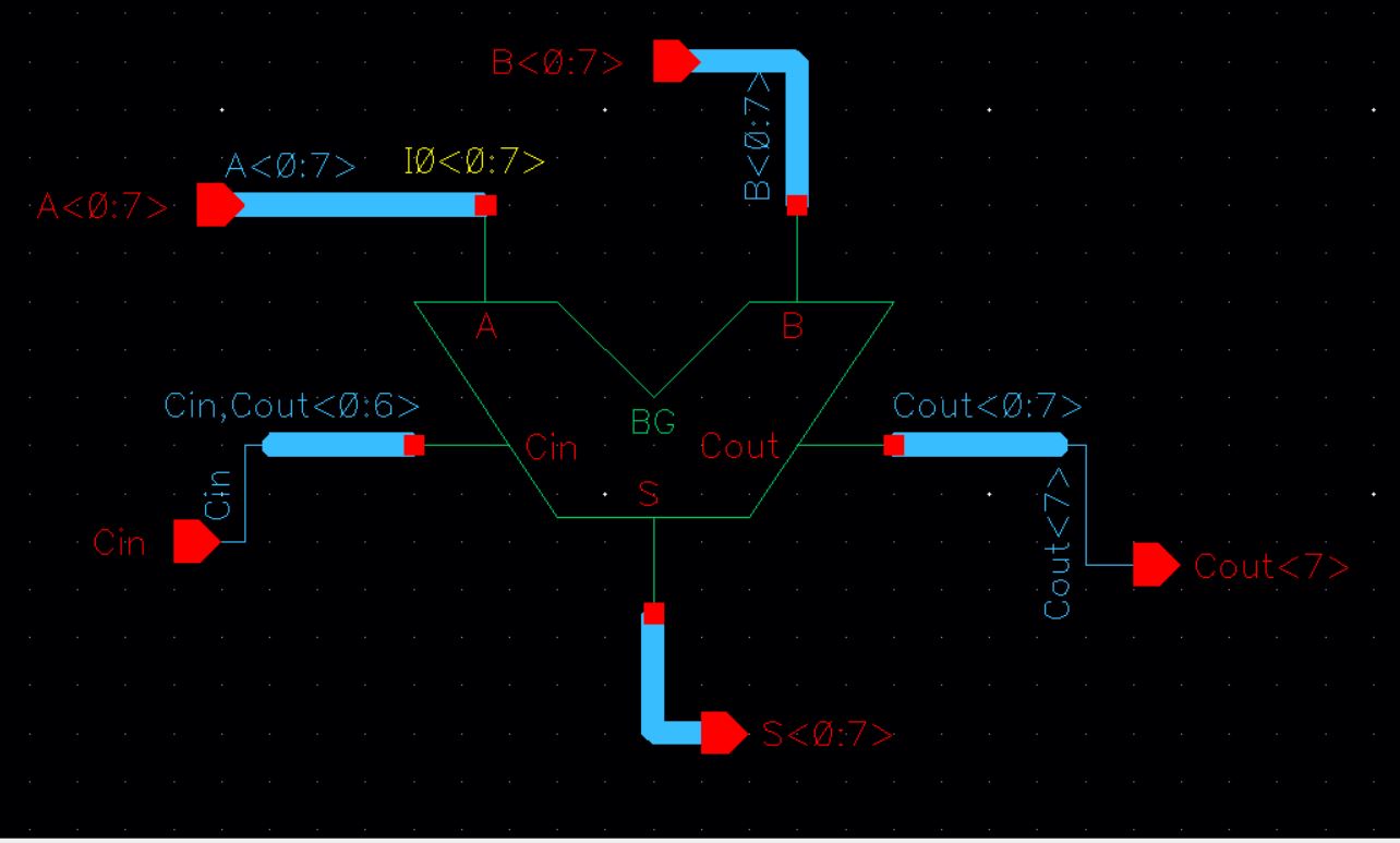
Schematic, Symbol layout, Extracted, DRC, LVS of AOI Full Adder
Schematic
Symbol
Layout and Extracted
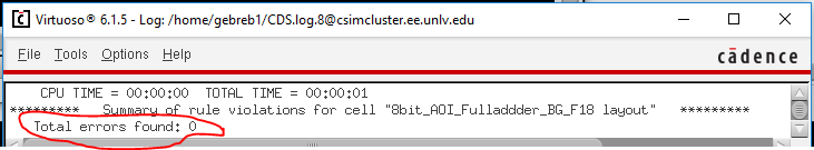
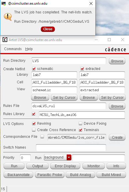
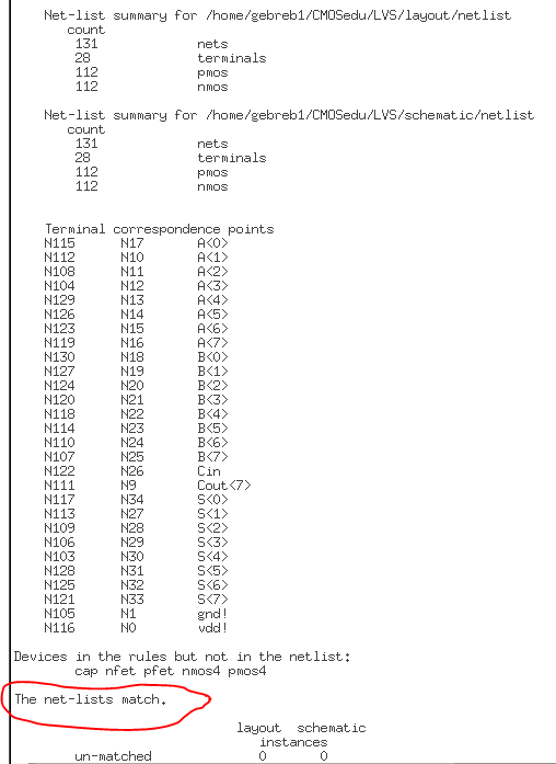
DRC and LVS
8-Bit AOI Full Adder Schematic,Simulation, Layout, Extracted, DRC and LVS
Schematic
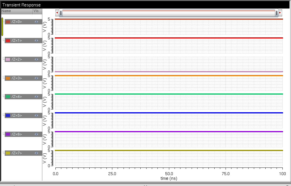
Simulation
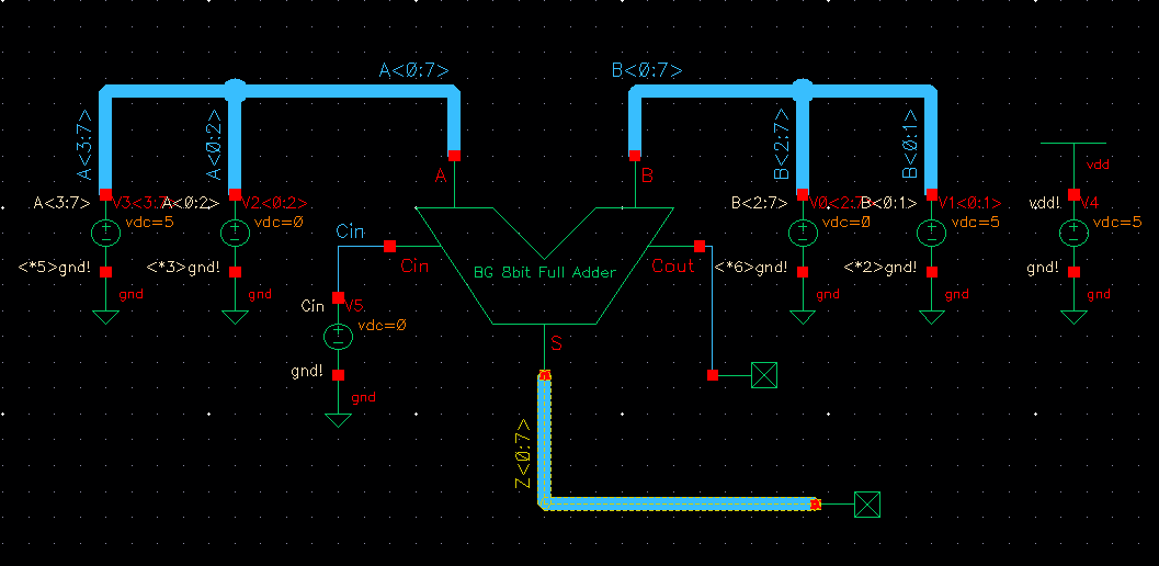
This
8 -bit full adder was tested by adding the number 00011111 from input A
and the number 11000000 from input B. The result as seen in the
simulation below is 11011111.
Layout and Extracted

DRC and LVS
The files, simulations, schematics, layouts, etc used in this lab can be downloaded in the link below.
Lab7_BG