Lab 6 - EE 421L
| 2-input NAND gate Schematic | 2-input NAND gate Symbol |
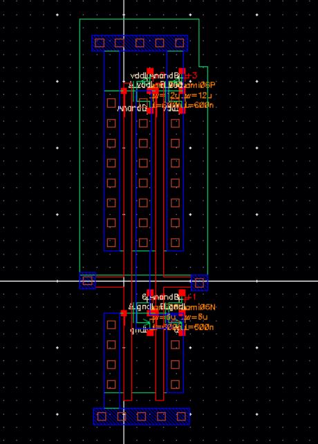
| 2-input NAND gate layout | 2-input NAND gate Extracted |
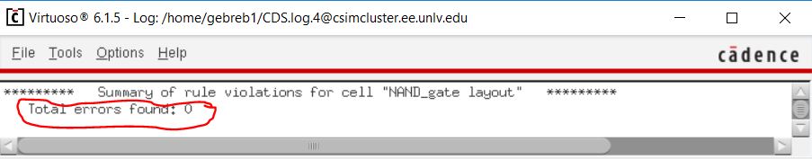
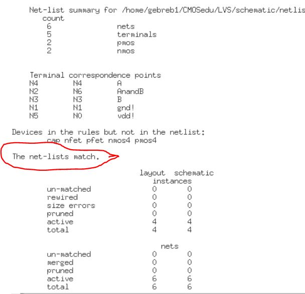
| 2-input NAND gate DRC | 2-input NAND gate LVS |
Design, layout,DRC, extract, and LVS a 2-input XOR gate
2- input XOR Schematic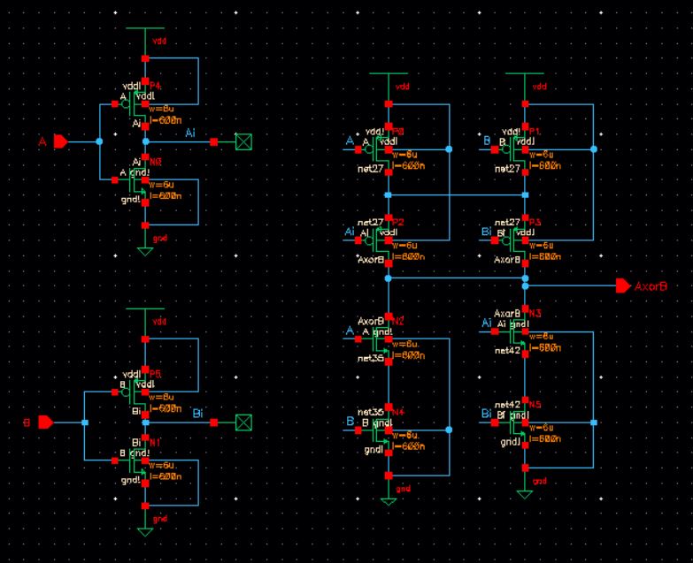 | 2-input XOR Symbol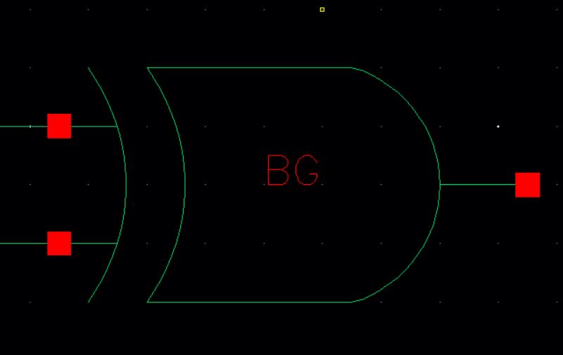 |
2-input XOR layout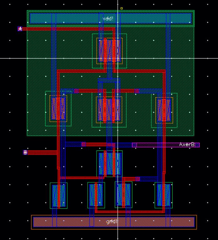 | 2-input XOR Extracted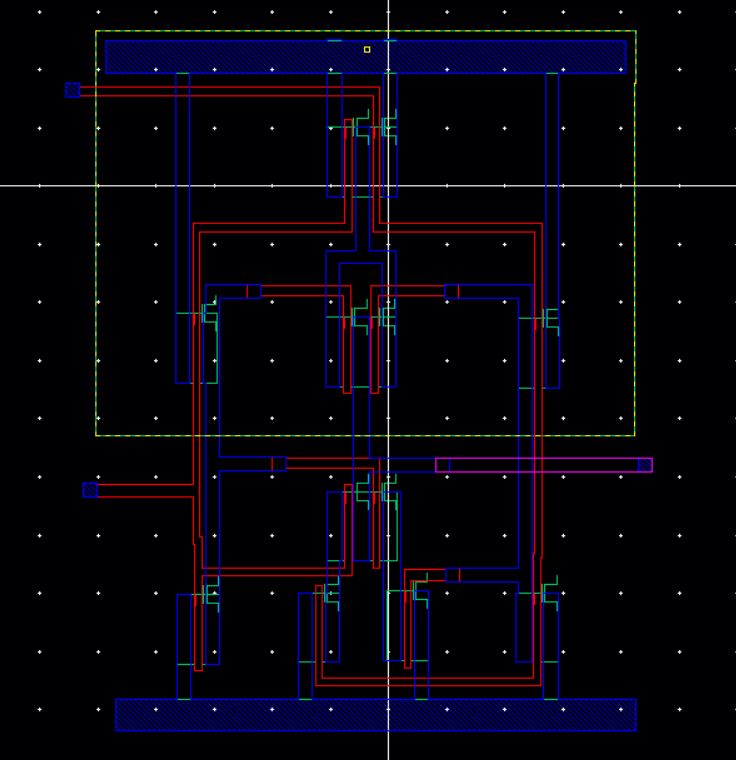 |
2-input XOR DRC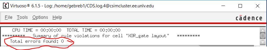 | 2-input XOR LVS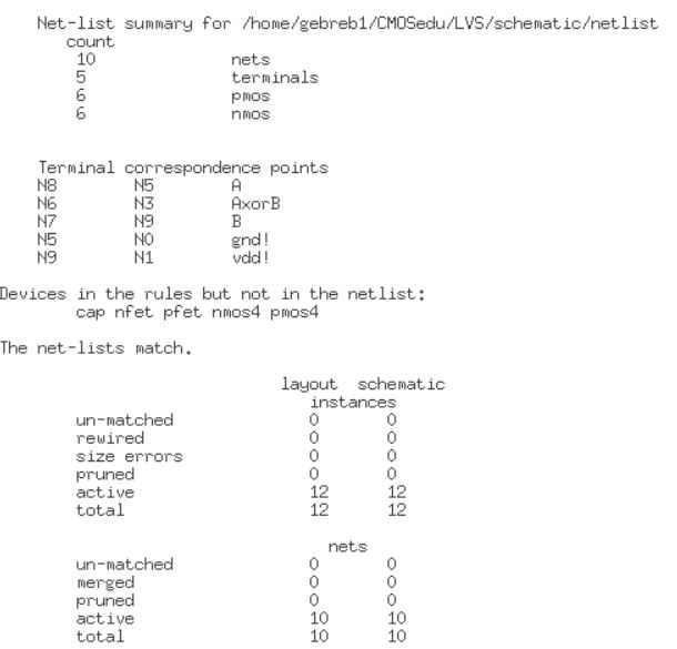 |
Exercise -3:
Simulations of NAND gate, XOR gate, and Inverter
NAND gate, XOR gate, and Inverter Schematic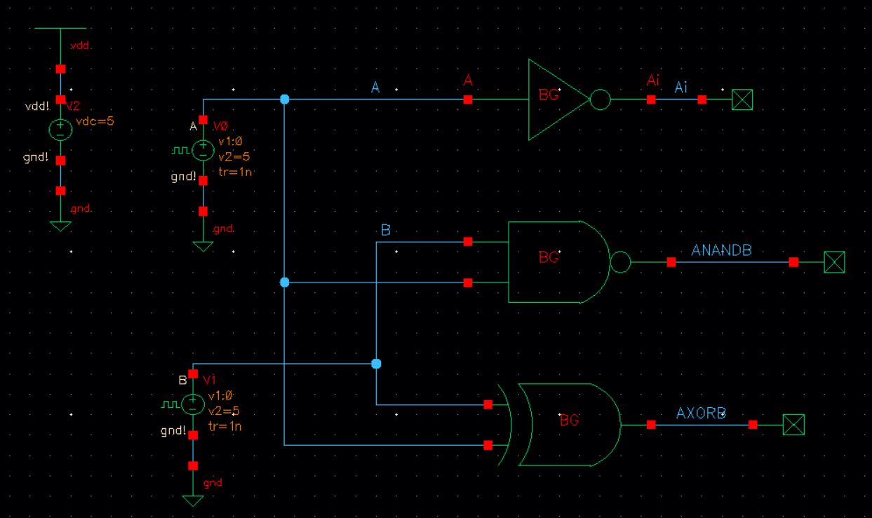 | NAND gate, XOR gate, and Inverter Simulation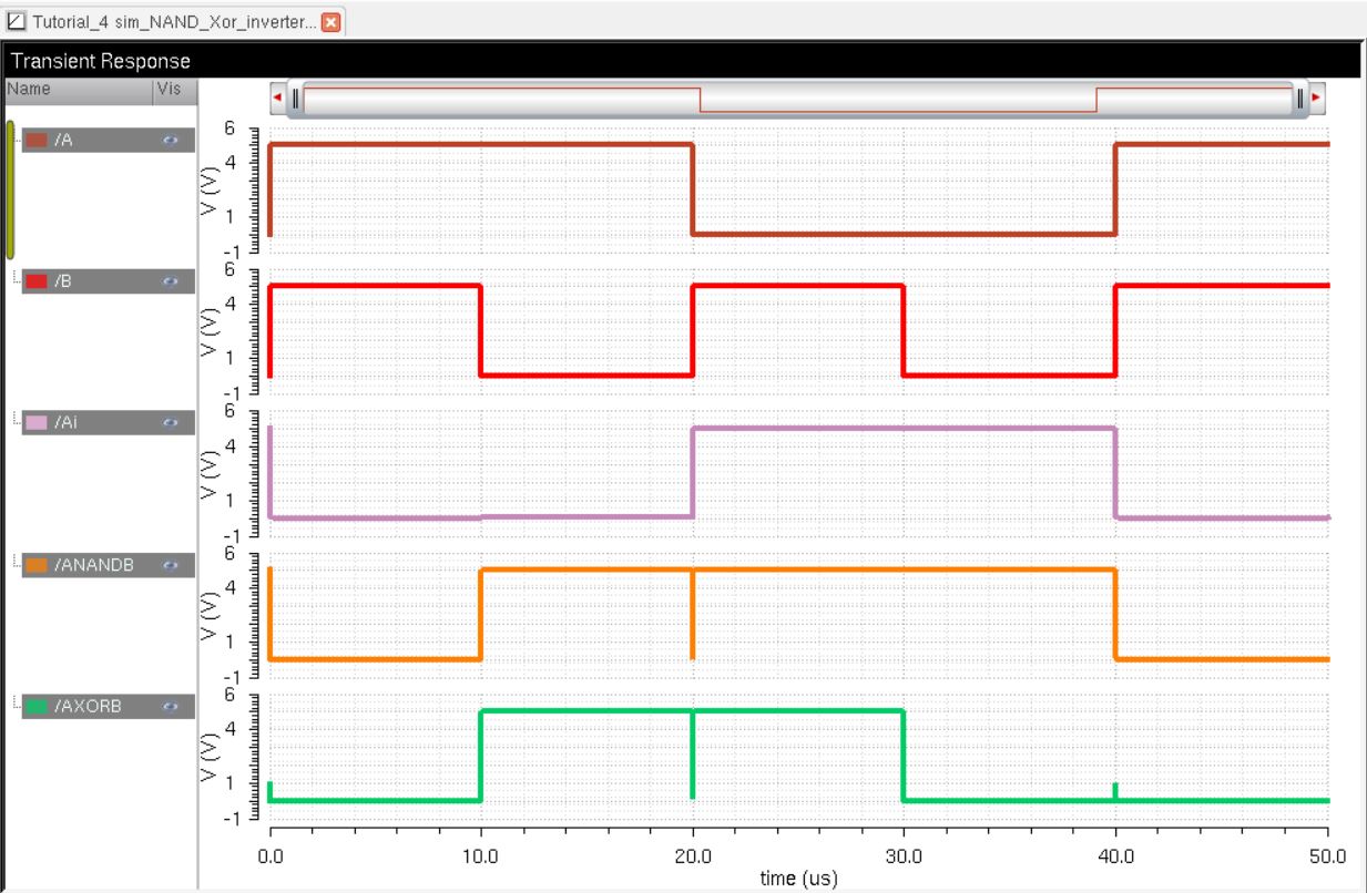 |
| A | B | A nand B | A xor B | |
| 0 | 0 | 1 | 0 | |
| 0 | 1 | 1 | 1 | |
| 1 | 0 | 1 | 1 | |
| 1 | 1 | 0 | 0 |
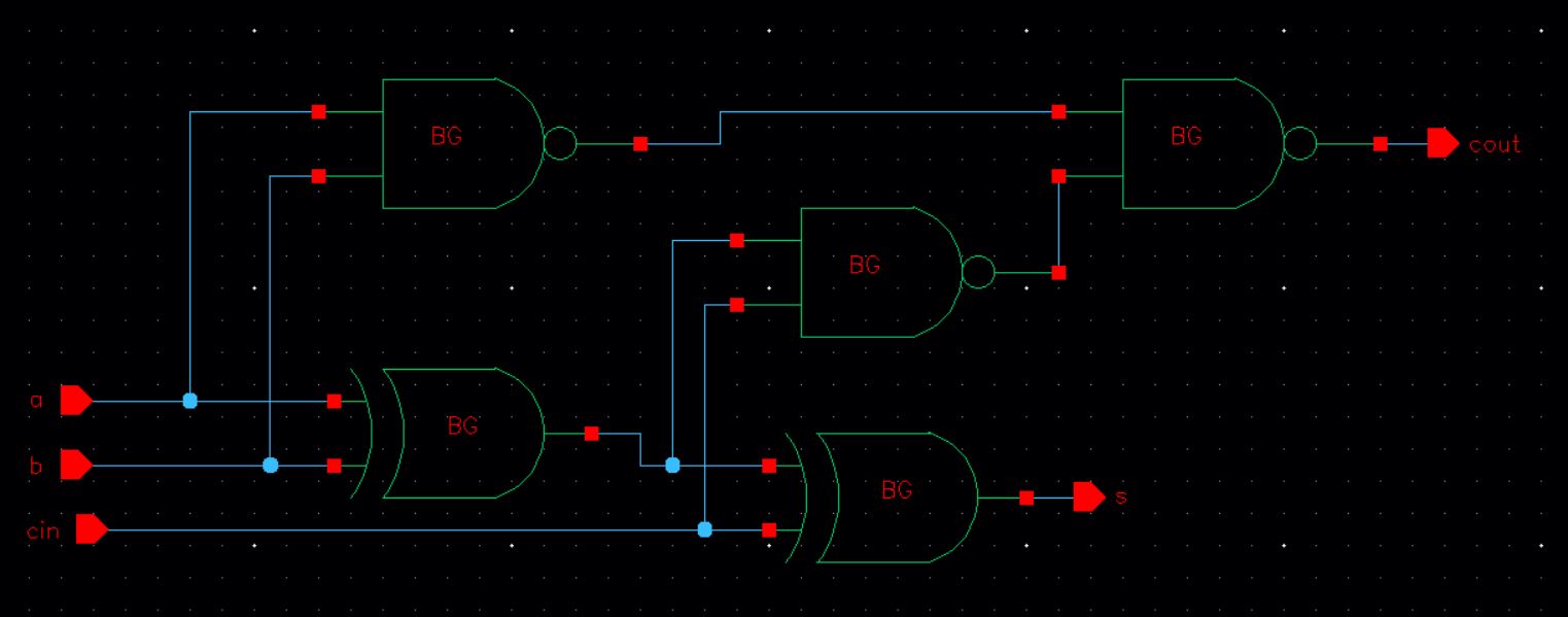
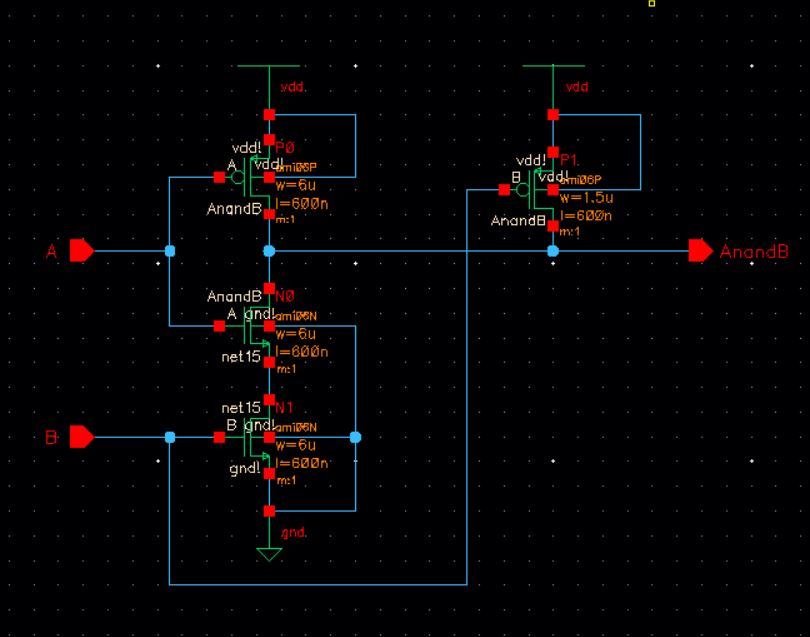
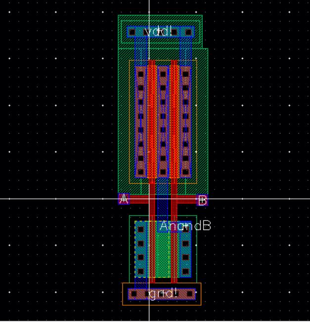
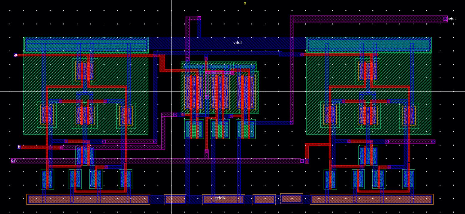
Full Adder Layout
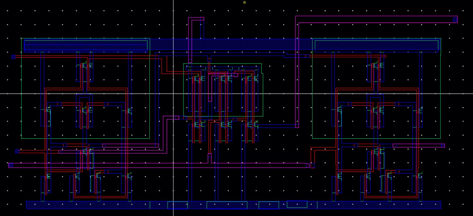
Full Adder Extracted
Full Adder DRC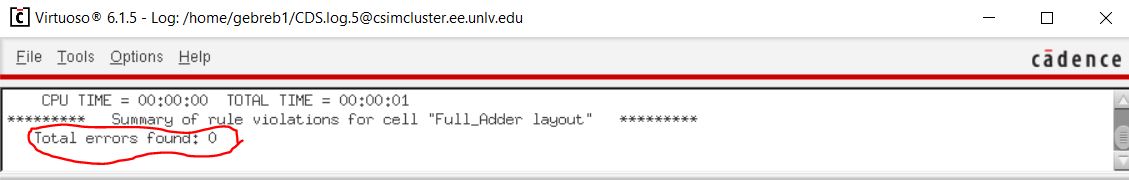 | Full Adder LVS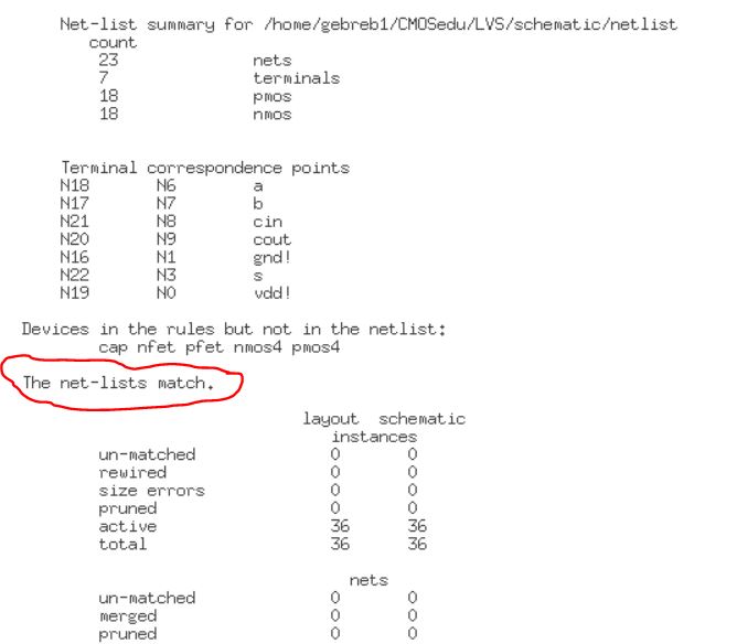 |
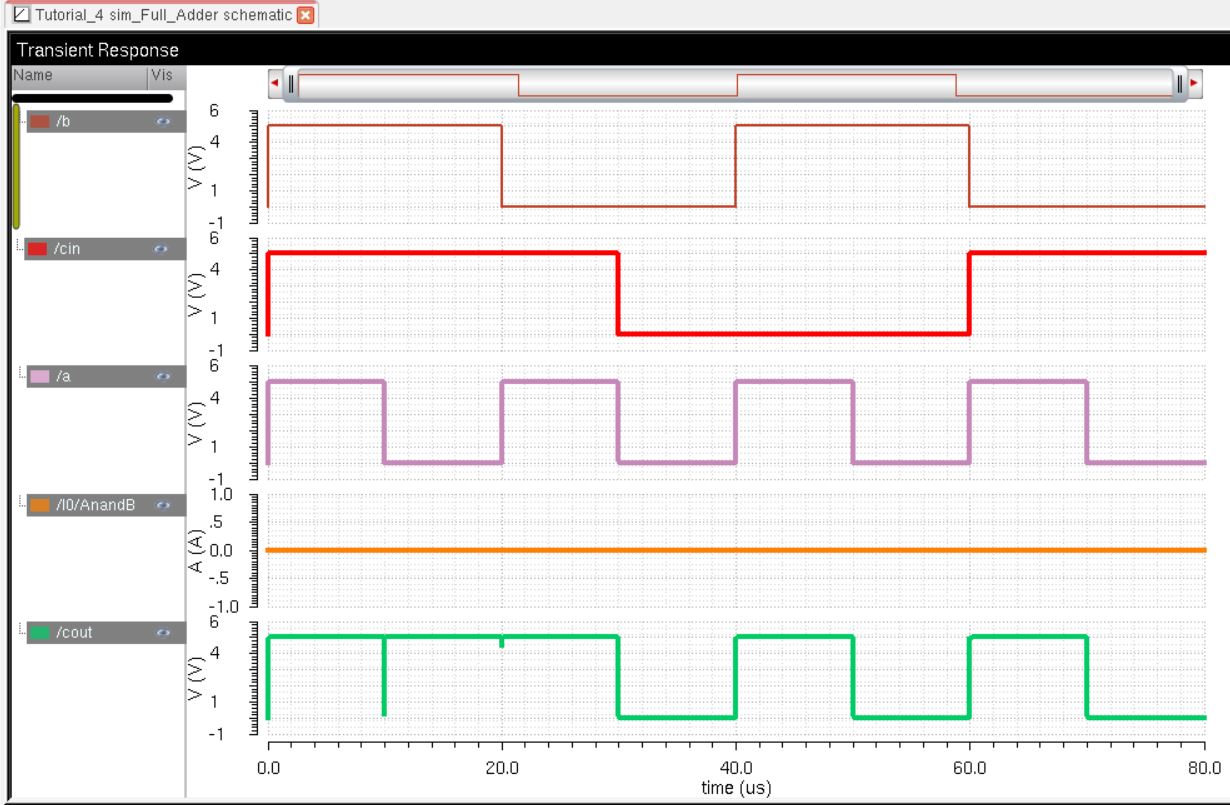
Full Adder Truth Table
| A | B | Cin | S | Cout |
| 0 | 0 | 0 | 0 | 0 |
| 0 | 0 | 1 | 1 | 0 |
| 0 | 1 | 0 | 1 | 0 |
| 0 | 1 | 1 | 0 | 1 |
| 1 | 0 | 0 | 1 | 0 |
| 1 | 0 | 1 | 0 | 1 |
| 1 | 1 | 0 | 0 | 1 |
| 1 | 1 | 1 | 1 | 1 |