Lab 5 - EE 421L
Authored
by Biruk Gebremeskel
Email: gebreb1@unlv.nevada.edu
October 10, 2018
Lab
description:
The purpose of this lab was to design, layout, and simulate a CMOS inverter.
Pre-Lab Work:
I backed up my work from my previous labs in my dropbox account.
I went through and finished Tutorial 3.
Actual Lab Work:
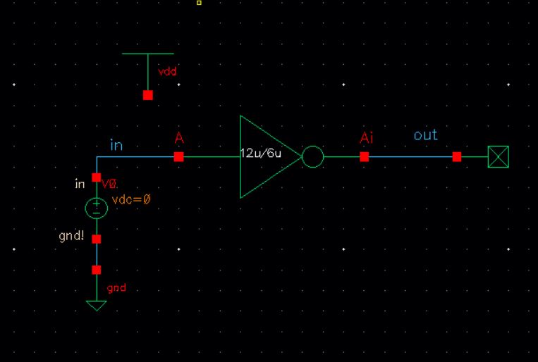
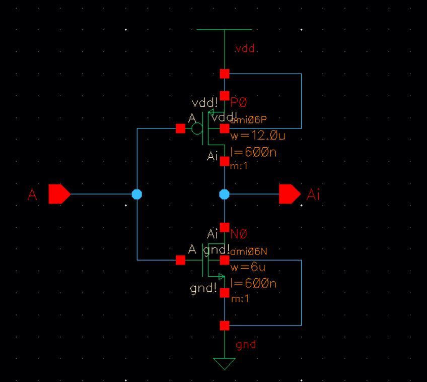
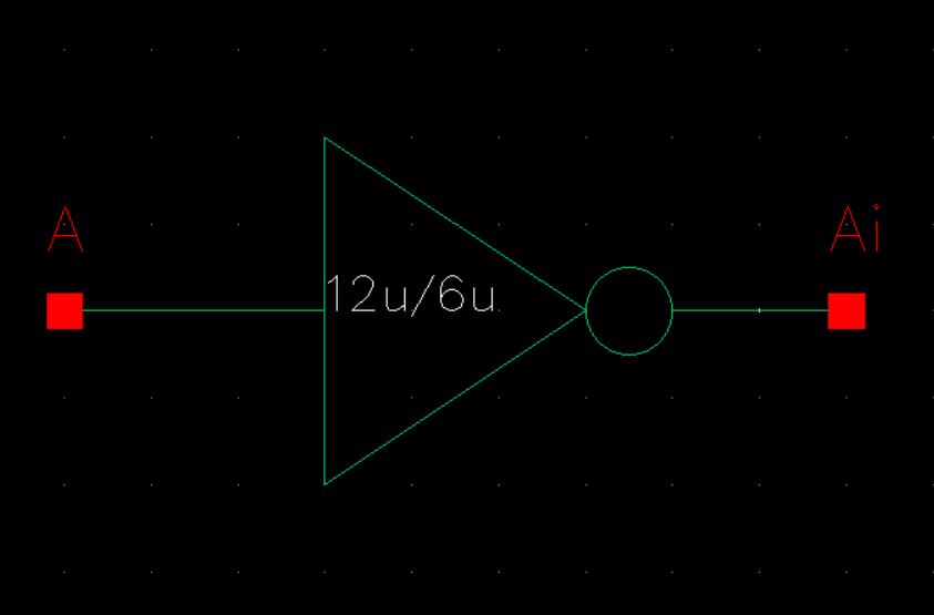
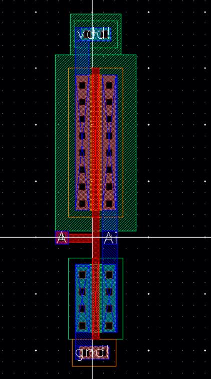
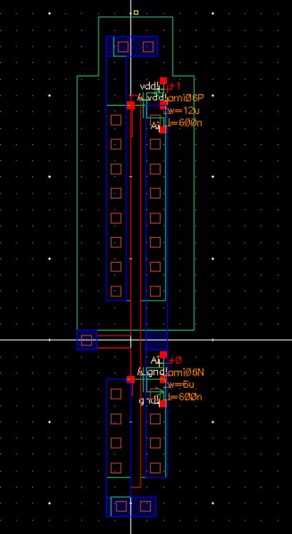
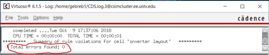
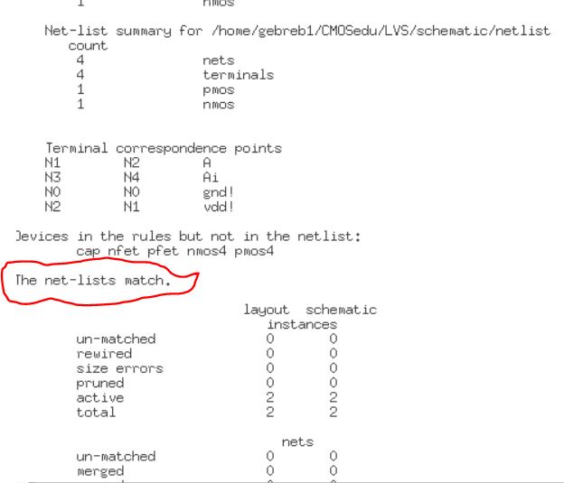
12u/6u Inverter( W of PMOS/W of NMOS):
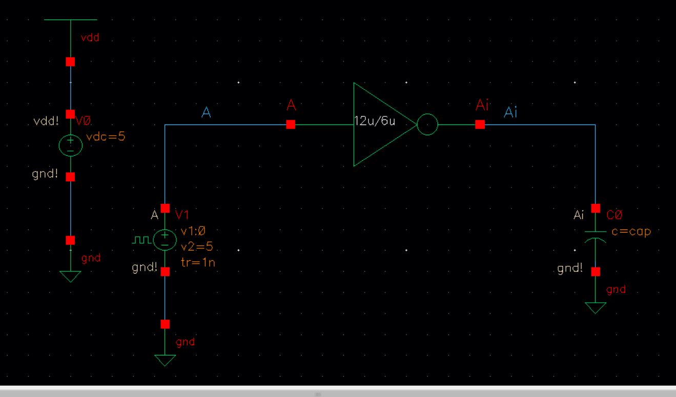
Schematic
 | Symbol
 |
Layout
 | Extracted
 |
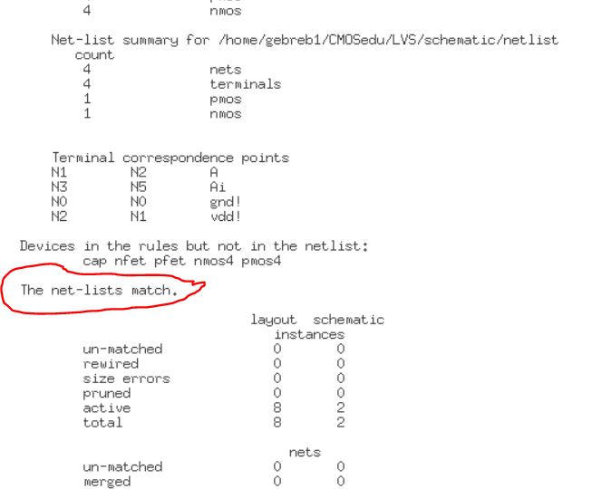
DRC
 | LVS
 |
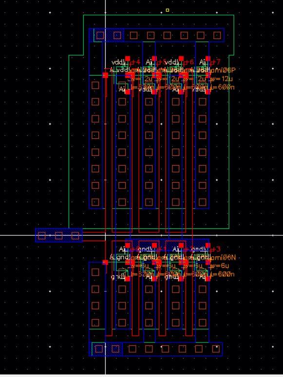
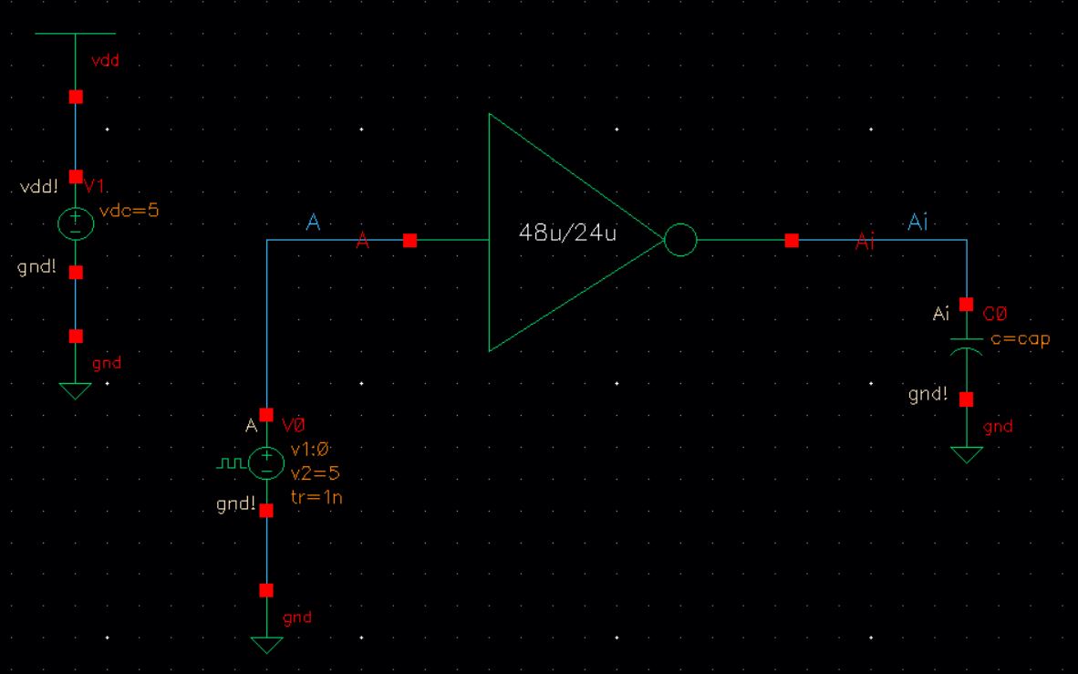
48u/24u Inverter ( i.e 12u/6u with M = 4):
Schematic
 | Symbol
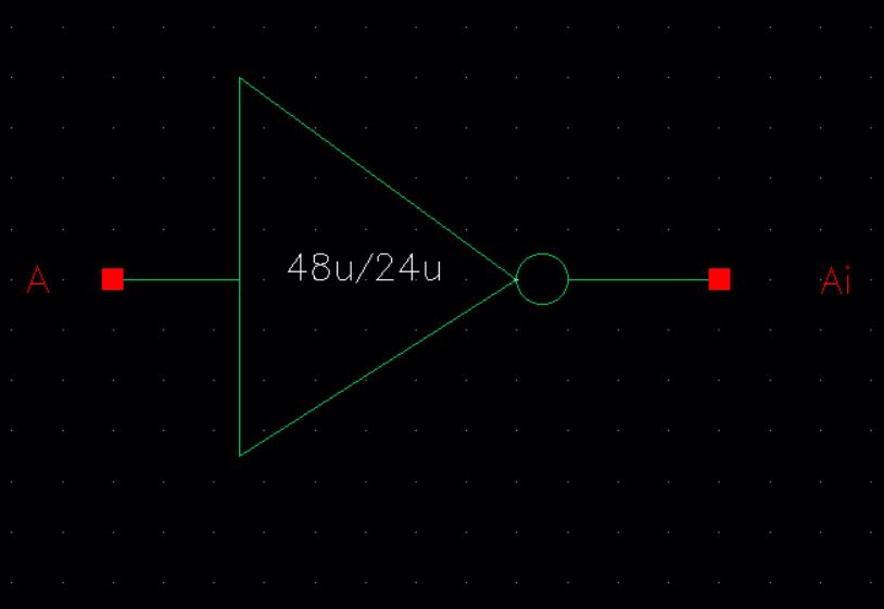 |
Layout
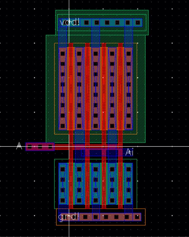 | Extracted
 |
DRC
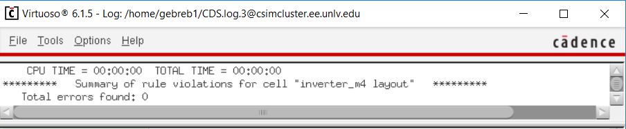 | LVS
 |
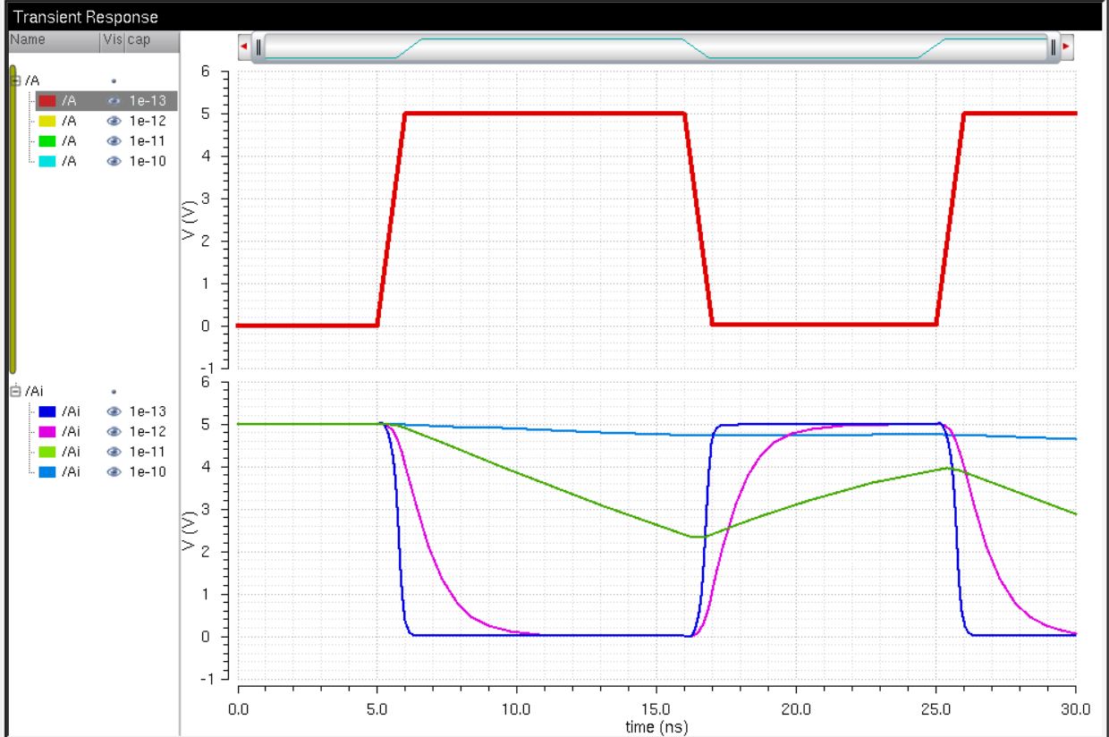
Simulations:
A
parametric analysis was performed to simplify and see the different
capacitive loads ranging from 100fF to 100pF with a total of 4
step size together.
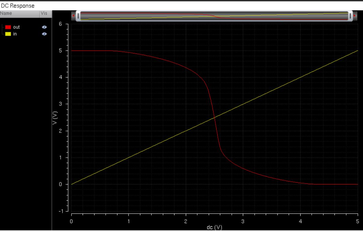
Spectre and UltraSim simulations of 12/6u inverter:
Schematic
 | Spectre Simulation
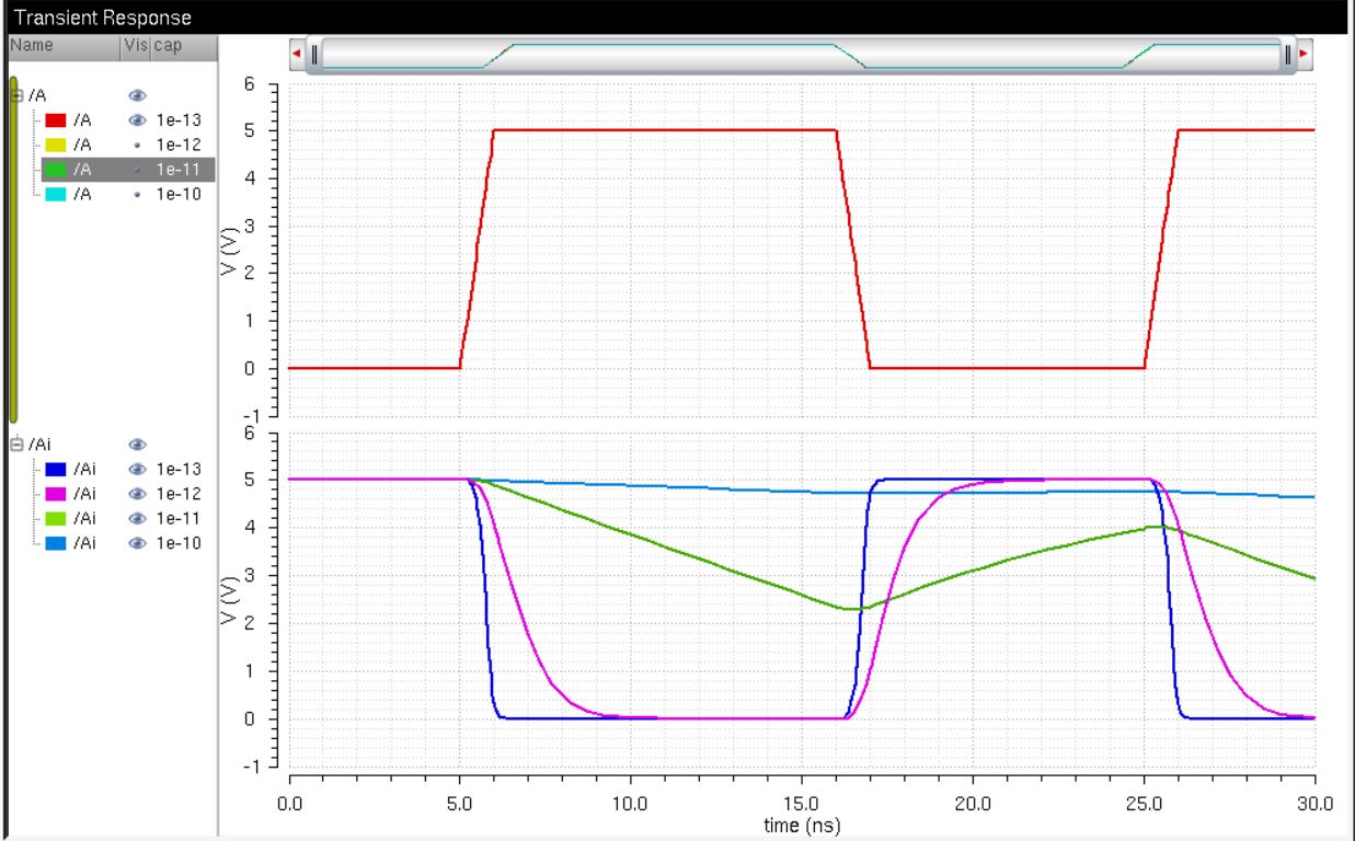 | UltrasSim Simulation
 |
Spectre and UltraSim Simulations of 48u/12u Inverter:
Schematic
 | Spectre Simulation
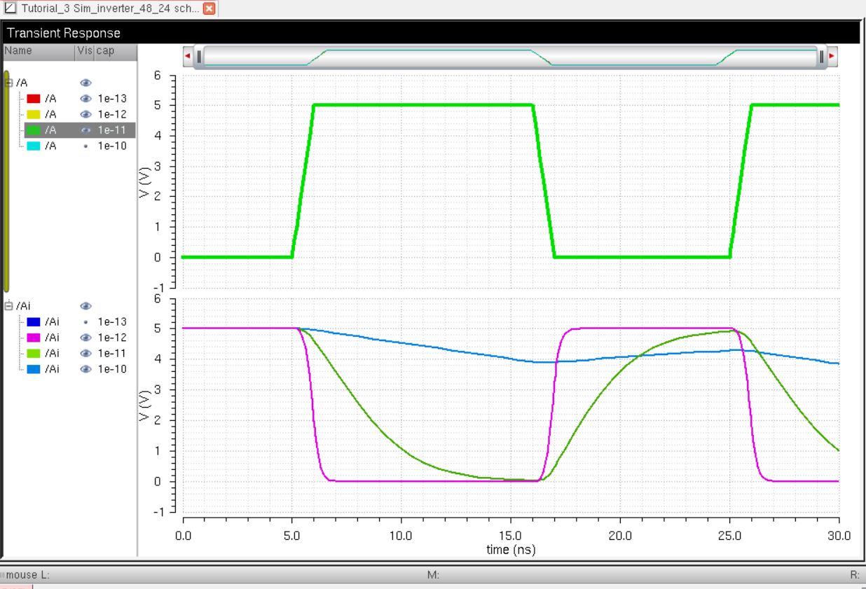 | UltraSim Simulation
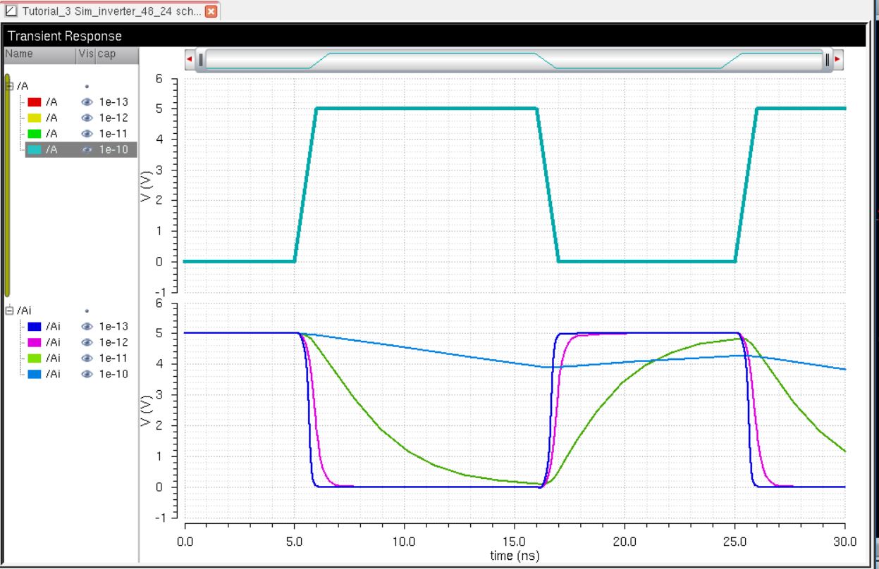 |
The cells used to generate the images used on this webpage can be found in lab5.zip
Return to Biruk's Labs
Return to EE421L F18 Student's Directory