Lab 4 - EE 421L
Authored
by Biruk Gebremeskel
Email: gebreb1@unlv.nevada.edu
September 26, 2018
Lab
description:
The purpose of this lab was to help us analyze IV characterstics and layout of NMOS and PMOS devices in ON's C5 process.
Pre-Lab Work:
I backed up my work from the previous labs and also went through Tutorial 2 before coming to the lab.
Actual Lab Work:
- A
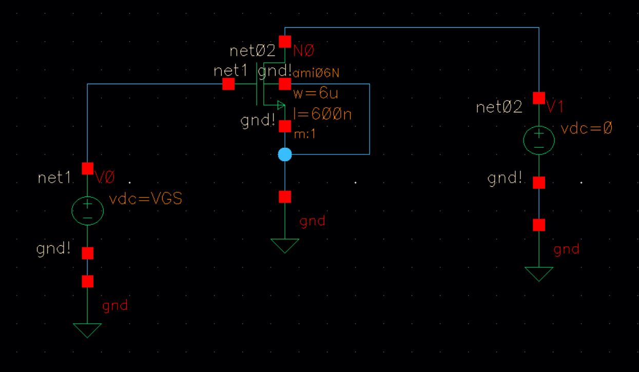
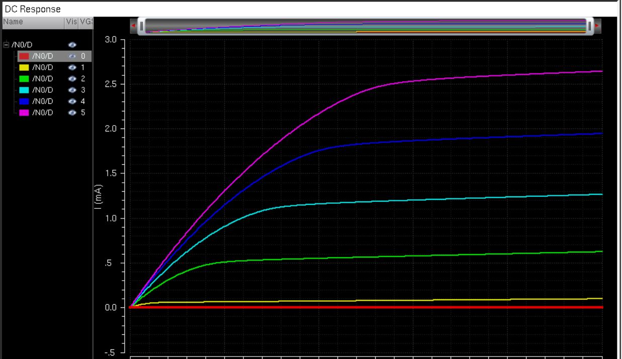
schematic for simulating ID v. VDS of an NMOS device for VGS varying from
0 to 5 V in 1 V steps while VDS varies from 0 to 5 V in 1 mV steps. Use a 6u/600n width-to-length ratio.
- A
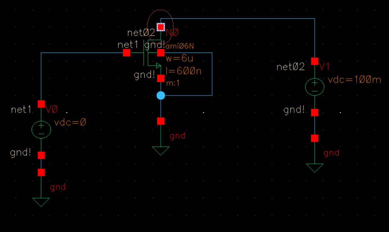
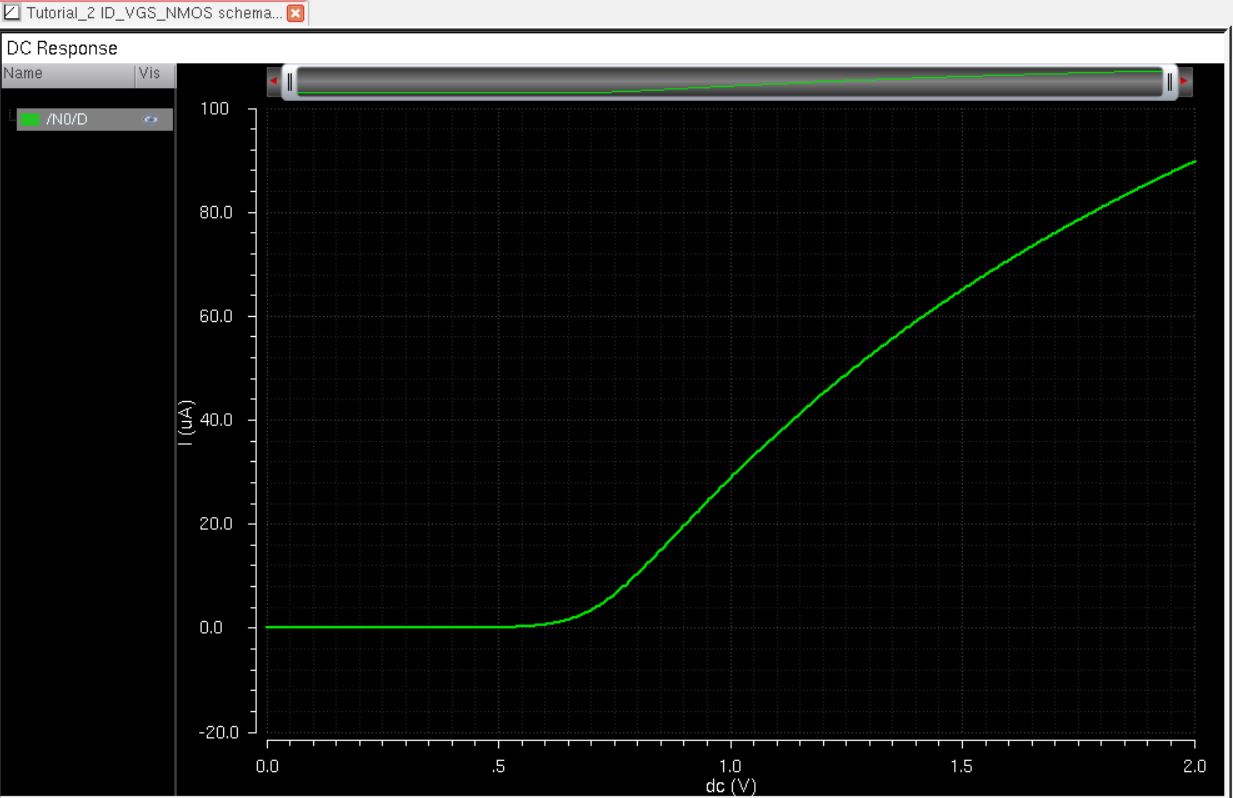
schematic for simulating ID v. VGS of an NMOS device for VDS = 100 mV
where VGS varies from 0 to 2 V in 1 mV steps. Again use a 6u/600n width-to-length ratio.
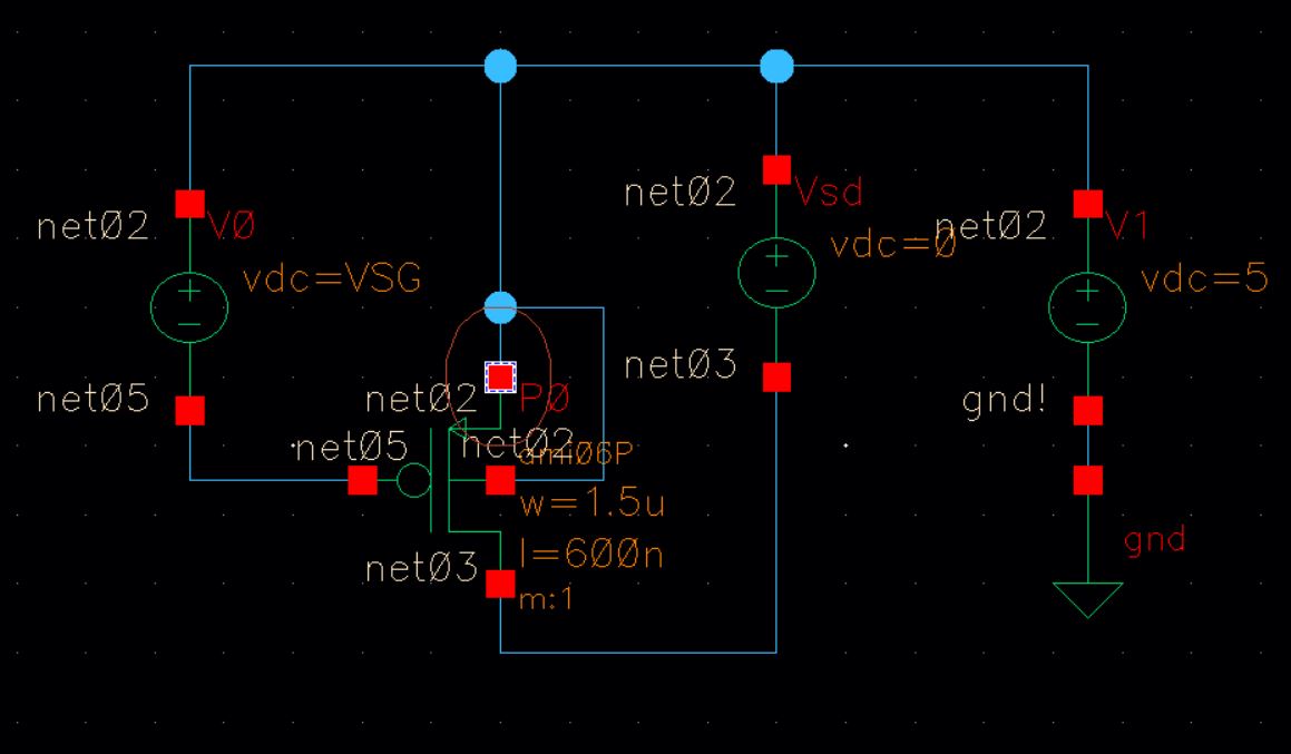
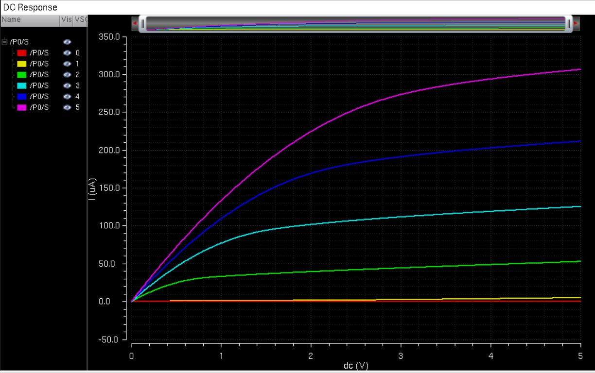
- A
schematic for simulating ID v. VSD (note VSD not VDS) of a PMOS device
for VSG (not VGS) varying from 0 to 5 V in 1 V steps while VSD varies
from 0 to 5 V in 1 mV steps. Use a
12u/600n width-to-length ratio.
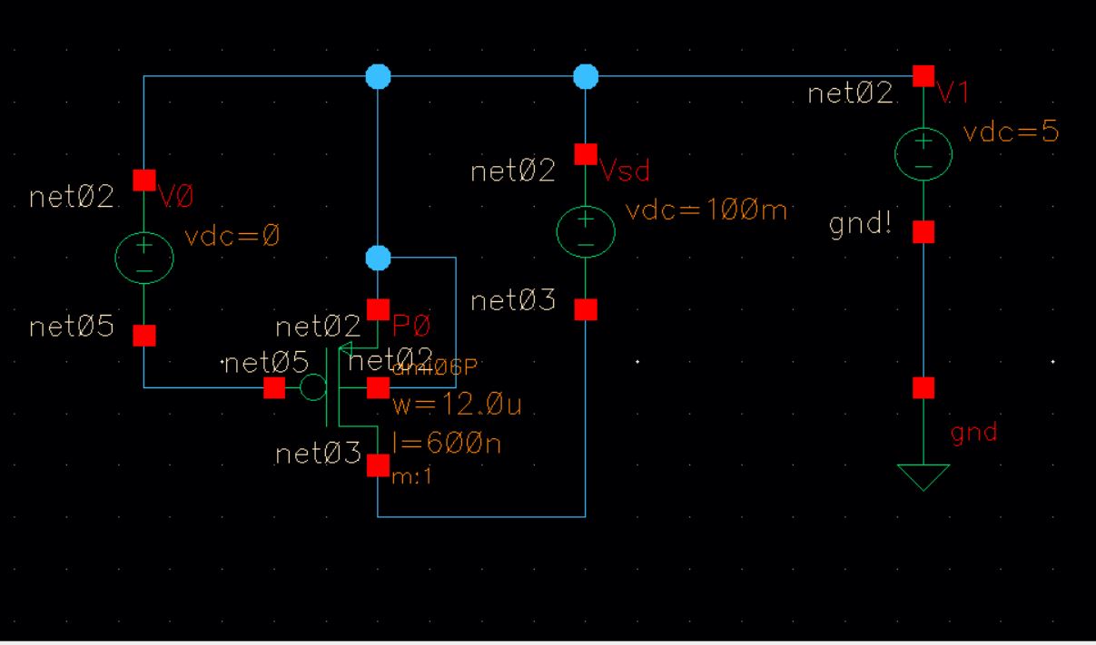
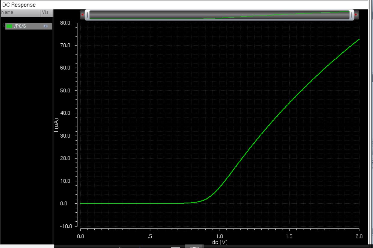
- A
schematic for simulating ID v. VSG of a PMOS device for VSD = 100 mV
where VSG varies from 0 to 2 V in 1 mV steps. Again, use a 12u/600n width-to-length ratio.
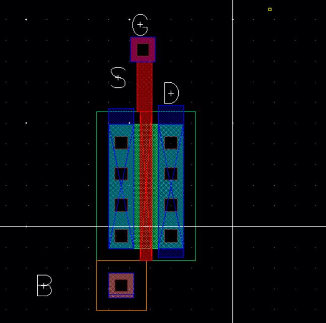
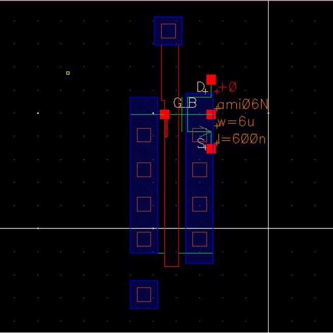
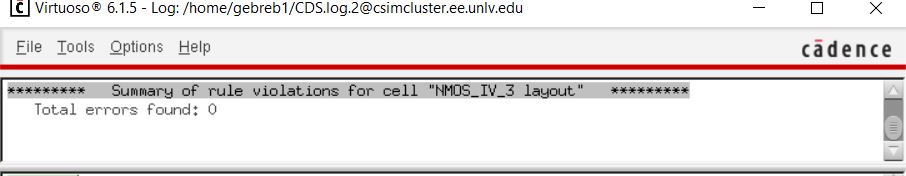
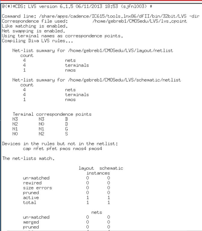
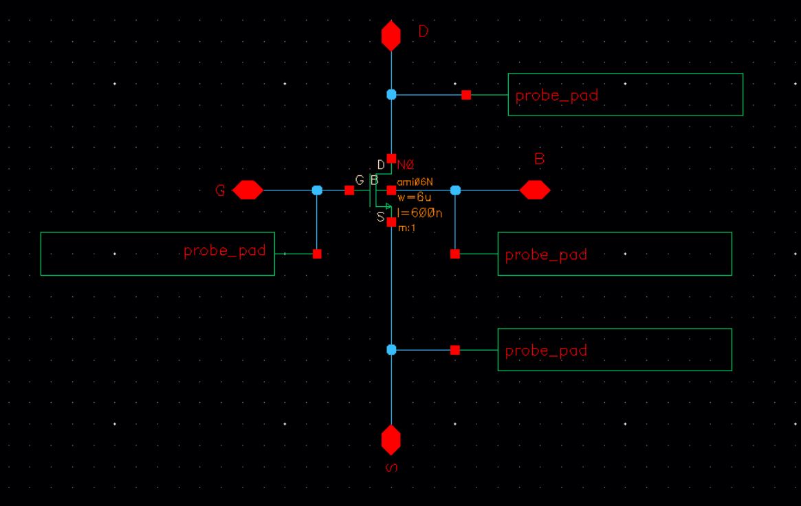
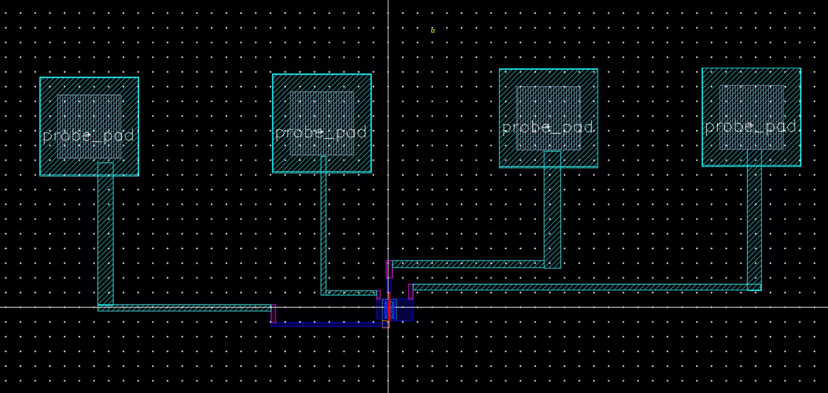
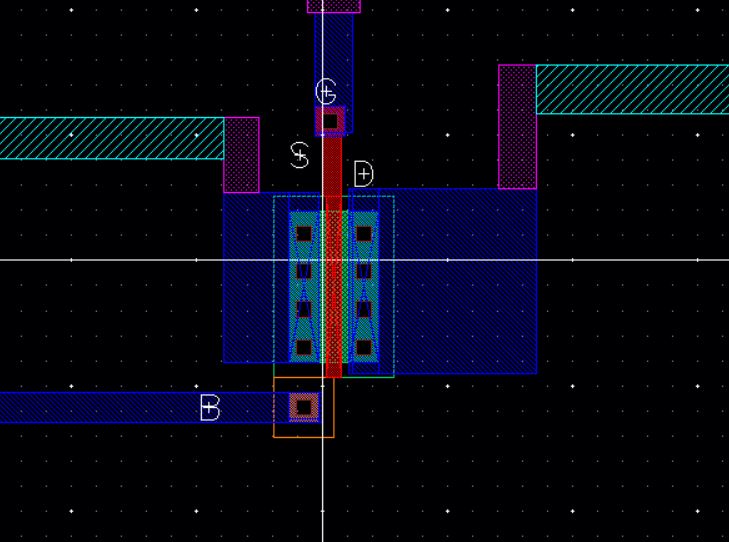
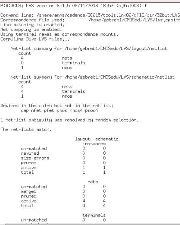
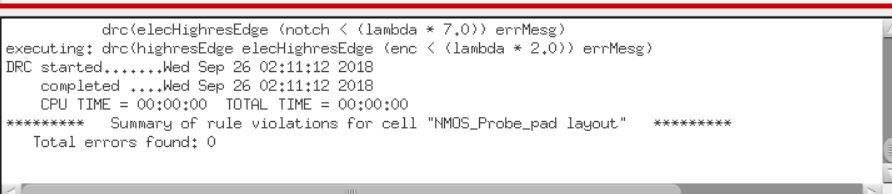
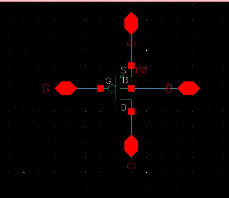
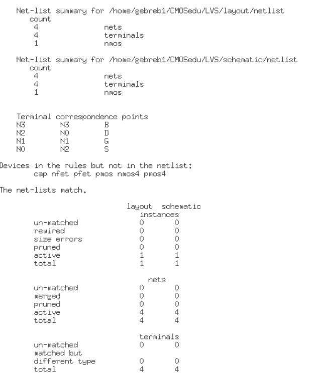
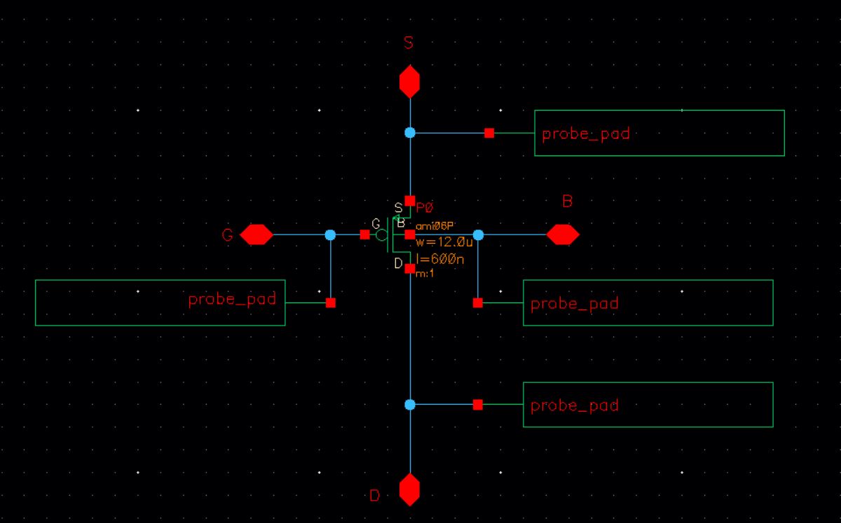
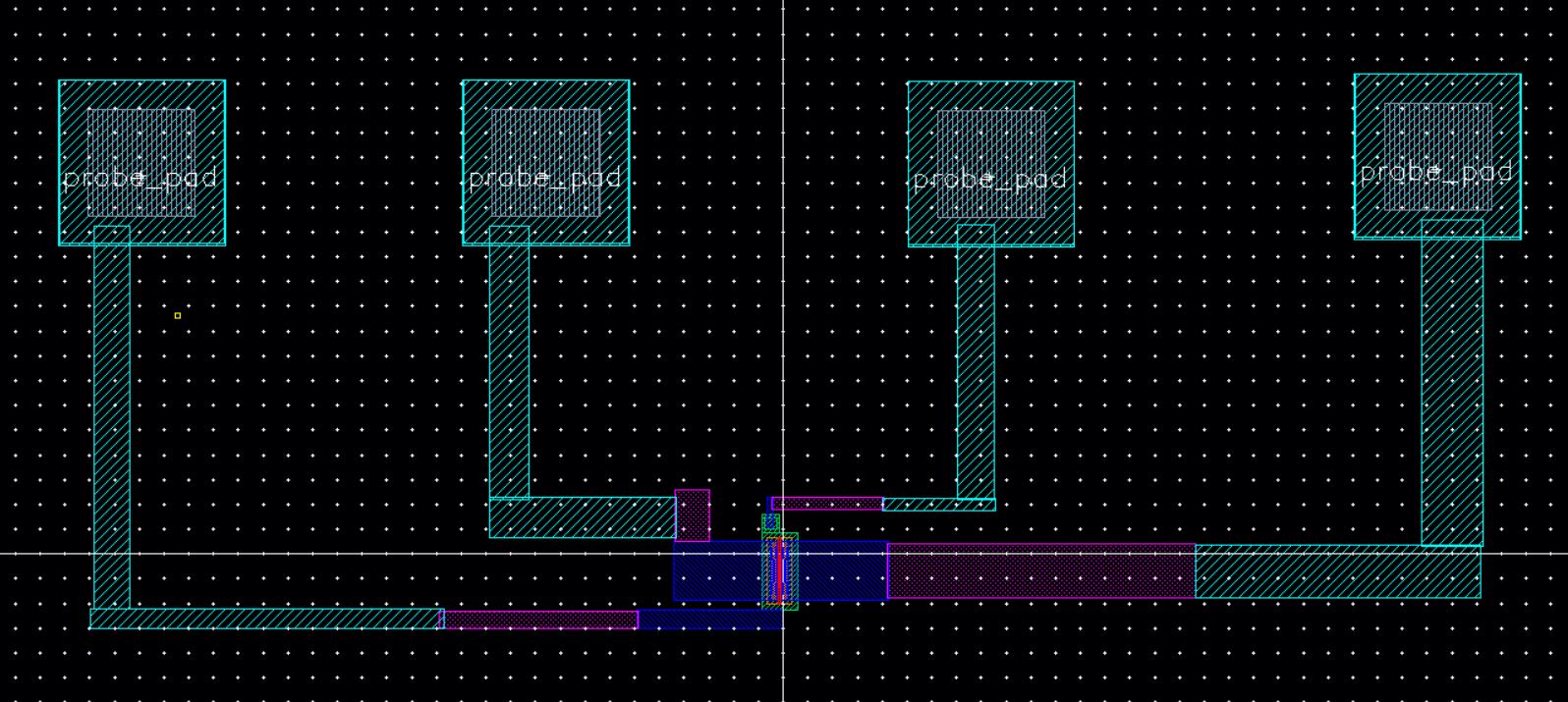
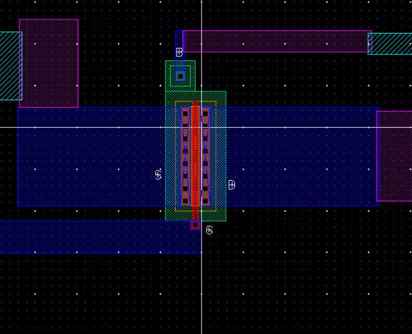
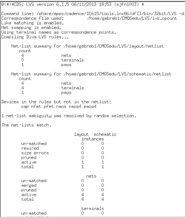
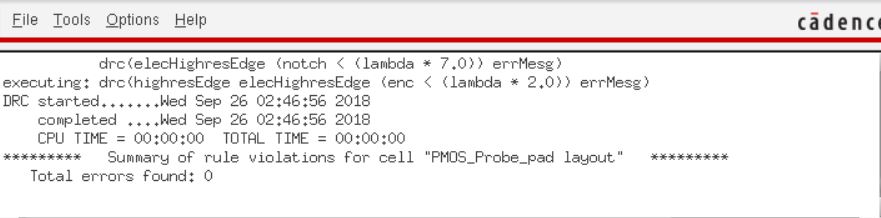
- Lay out a
6u/0.6u NMOS device and connect all 4 MOSFET terminals to probe pads
(which can be considerably smaller than bond pads [see MOSIS design rules]
and directly adjacent to the MOSFET (so the layout is relative small).
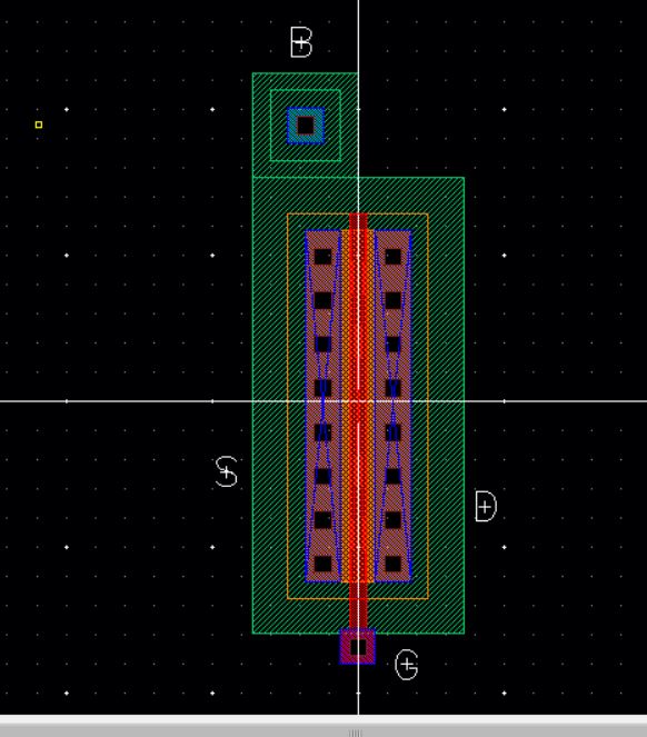
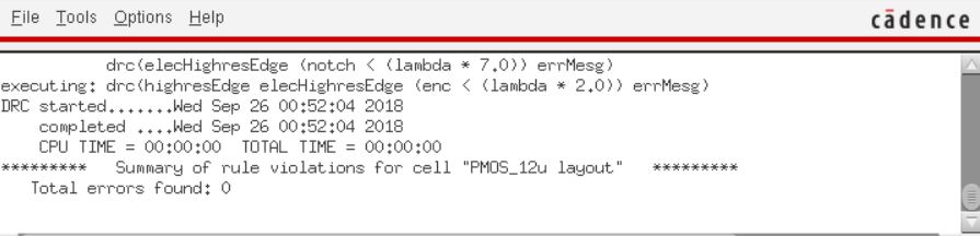
- Lay out a
12u/0.6u PMOS device and connect all 4 MOSFET terminals to probe pads.


Return to Biruk's Labs
Return to EE421L F18 Student's Directory