Lab 3 - EE 421L
Authored
by Biruk Gebremeskel
Email: gebreb1@unlv.nevada.edu
Septemeber 19, 2018
Lab
description:
The
purpose of this lab was to do the layout of the 10-bit digital to
analog converter (DAC) that we designed in the previous lab.
Pre-lab work:
I made sure that i backed-up all my previous lab works before coming to this lab and also finished watching Tutorial 1.
Post-lab work:
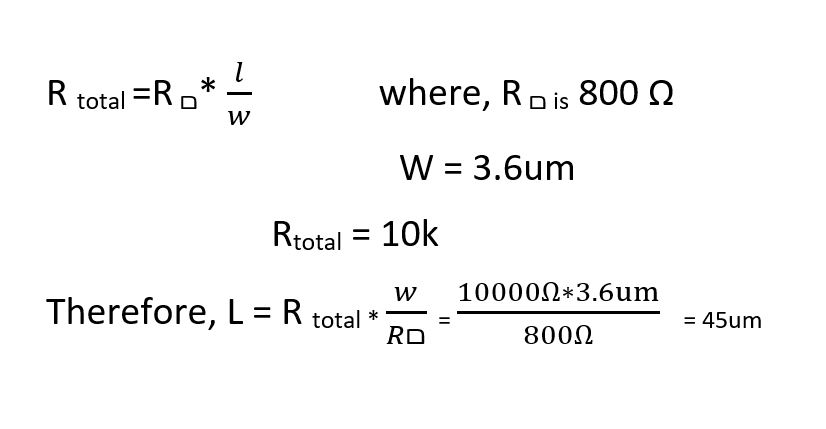
I used the n-well to layout a 10k resistor as discussed in Tutorial 1.
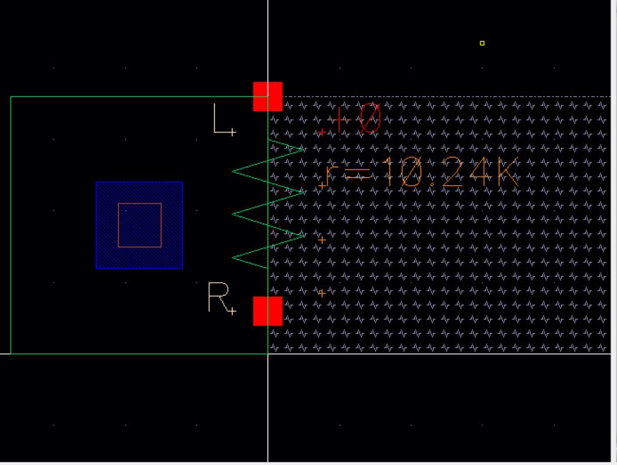
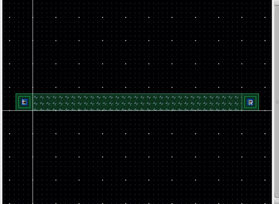
In
order to make a 10k resistor using n-well i calculated the length of
the n-well needed using the formula below while taking 3.6um for
the width because that is the minimum we can go by referring into MOSIS.
I used the above n-well resistor to create the layout of my 10-bit DAC
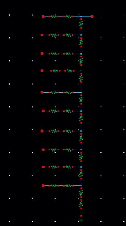
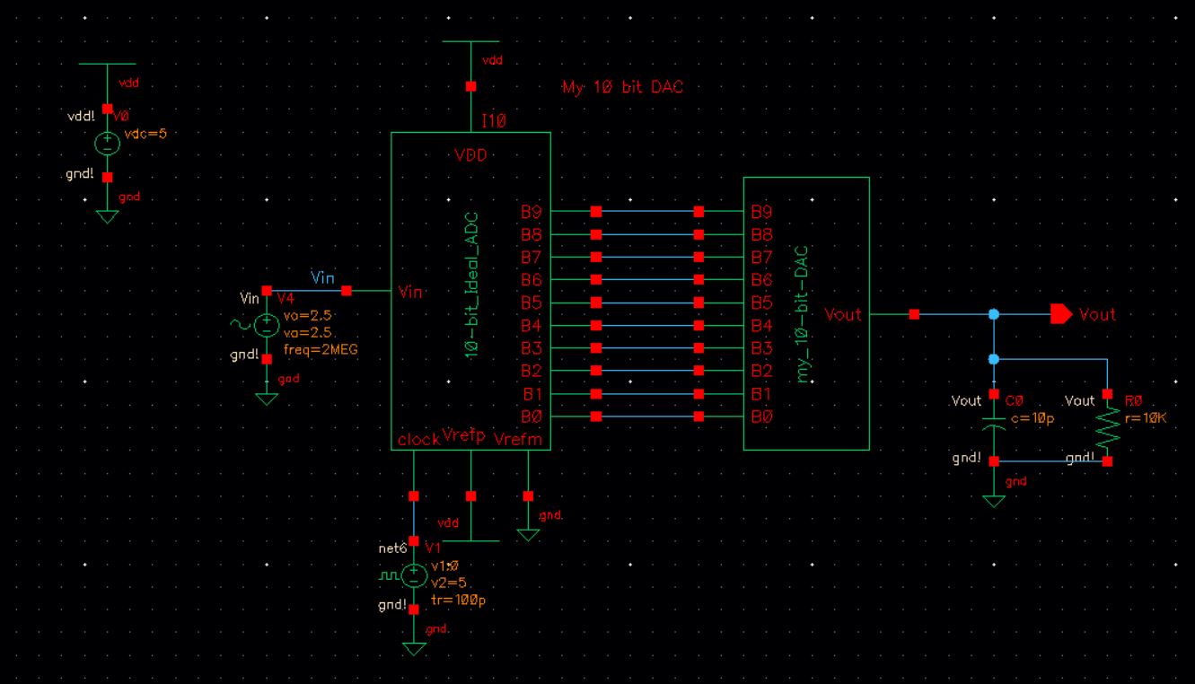
my schematic from the previous lab:
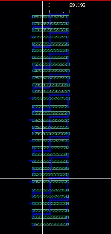
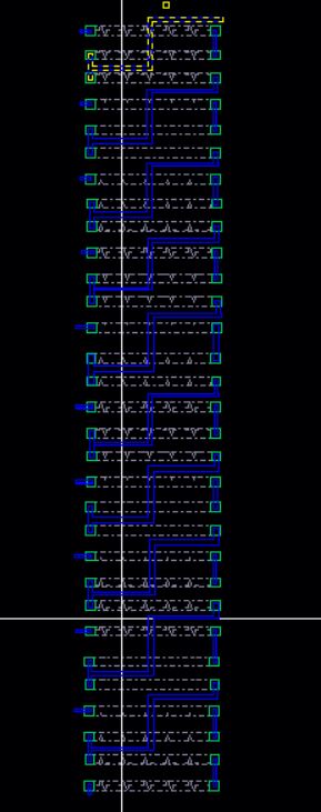
The layout i created using the above schematic:
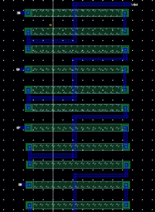
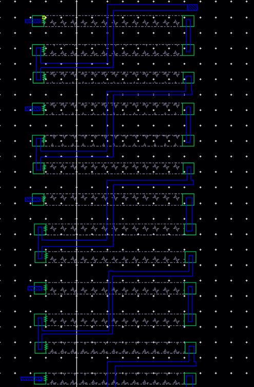
The extracted file:
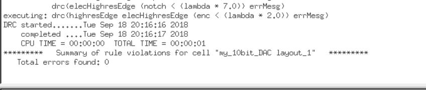
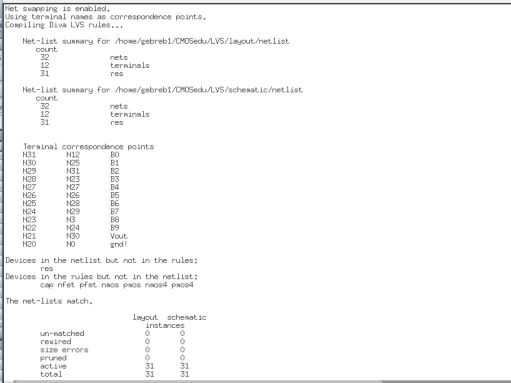
The LVS:
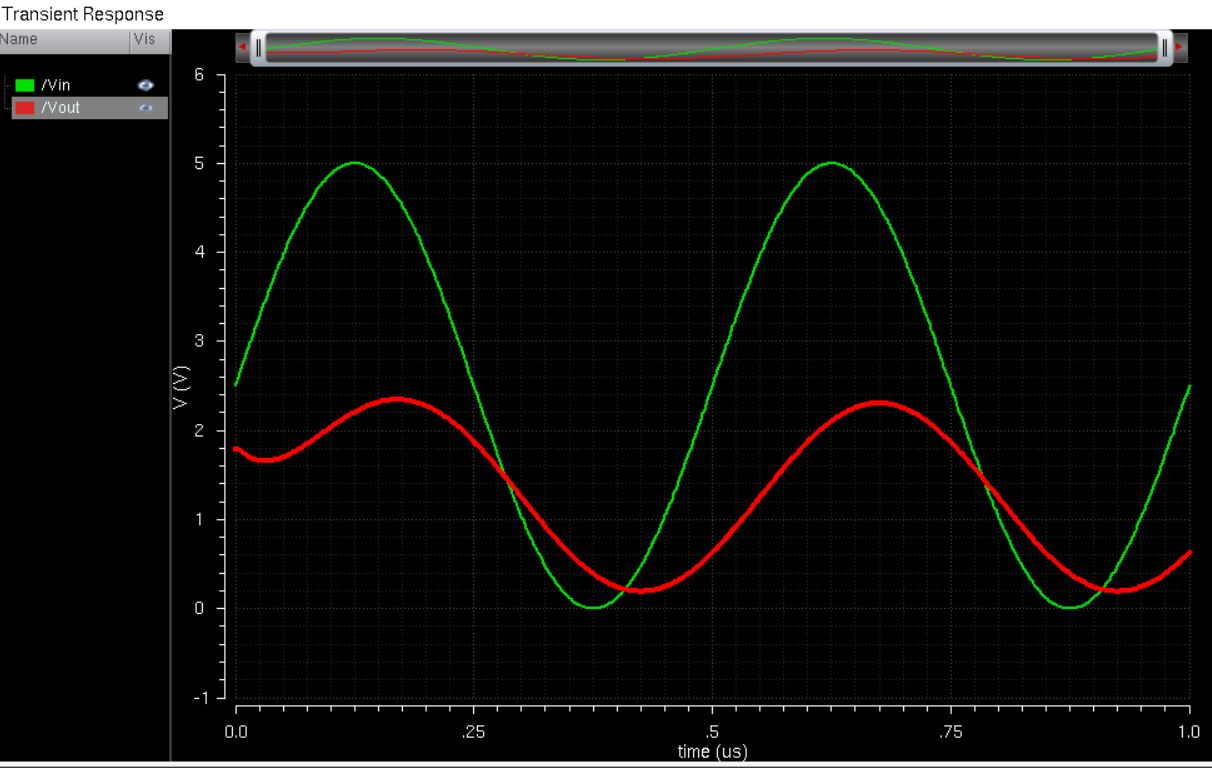
Simulation of the layout:
The ideal_ADC_DAC schematic with the DAC replaced by the 10-bit DAC i designed in lab2.
I attached my final design directory below.
Lab3.files
Return to Biruk's labs
Return to EE421l F18 Student's Directory