Lab 2 - EE 421L
Authored
by Biruk Gebremeskel
Email: gebreb1@unlv.nevada.edu
September 13, 2018
Lab
description:
The purpose of this lab was to design a 10-bit digital to Analog converter (DAC).
Pre-lab Work:
In
this pre-lab, after reading the entire write-up posted in the website,
I followed the steps listed to tell us what is required to be done.
Therefore,
I first downloaded lab2.zip file to my desktop and then I
uploaded it to my design directory server, CMOSedu directory. Then
after, I unziped the directory using the command, unzip lab2.zip, in
Cadence and added the DEFINE statement( i.e DEFINE lab2$
HOME/CMOSedu/lab2) in cds.lib.Since I completed the above steps, I was
able to navigate and find the lab2 library in the library directory and
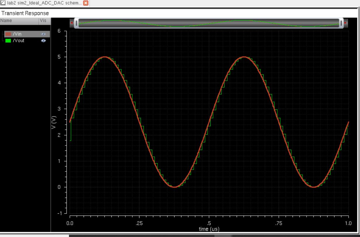
open the schematic view of the cell sim_Ideal_ADC_DAC.
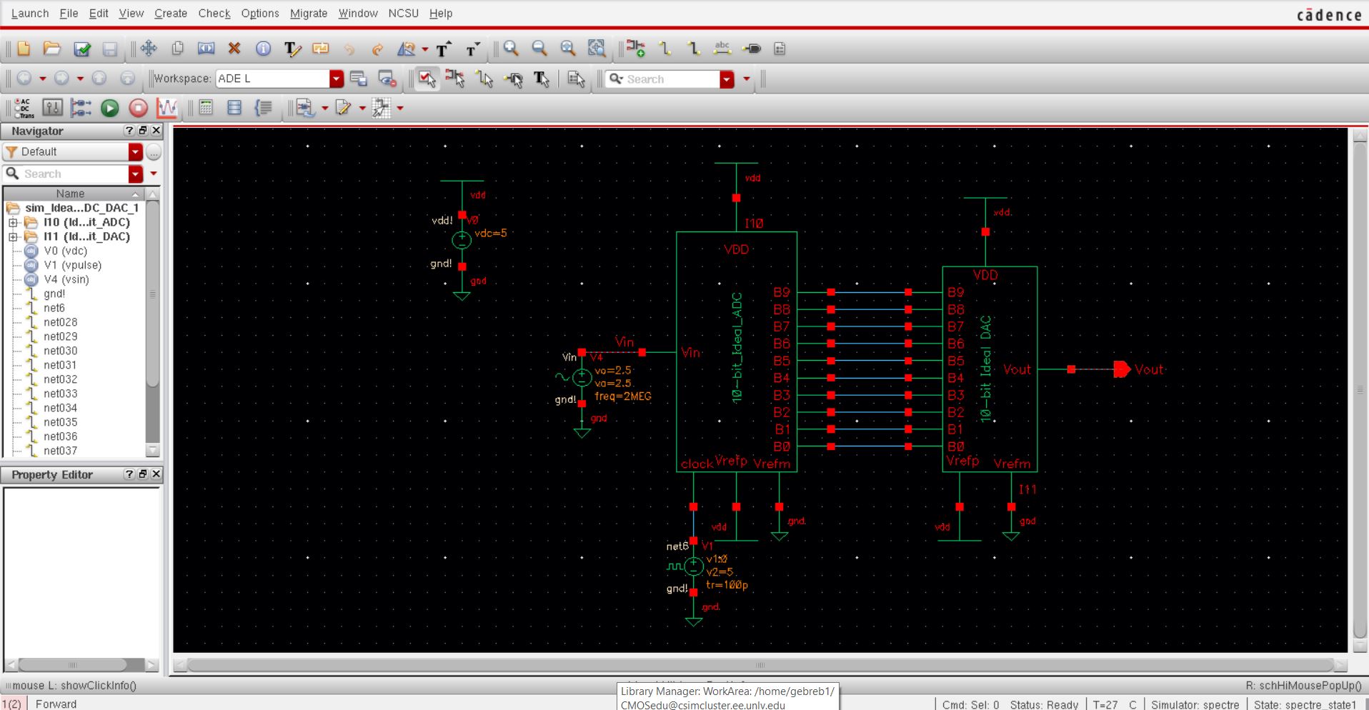
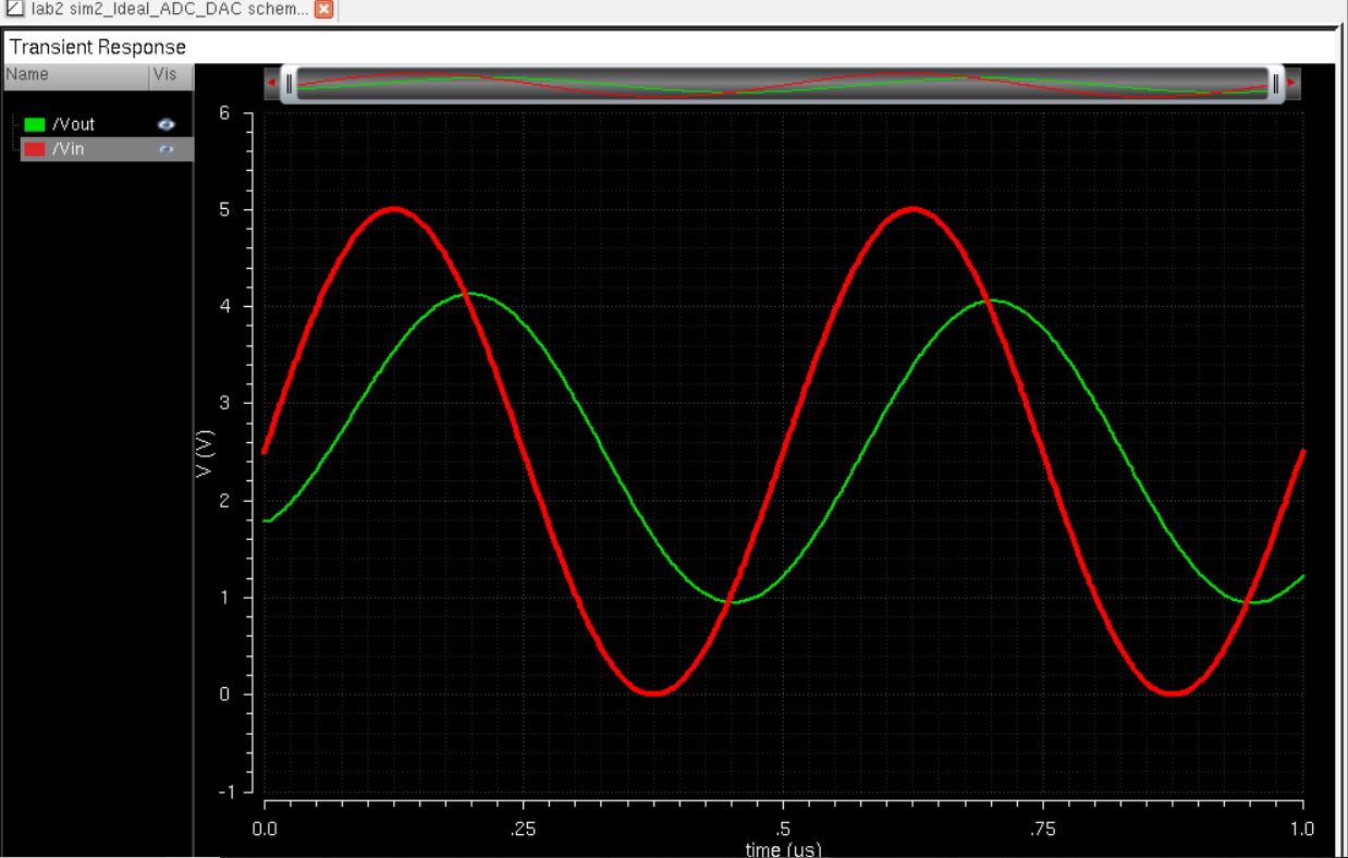
As
we seen above in the simulation the input which is a digital signal in
this case is converted into an analog output by the DAC. This is a very common applications to store and play audio signals.
The value of the least significant bit is calculated using the formula bleow.
1 LSB = Vdd/2^(n)
Post-Lab work:
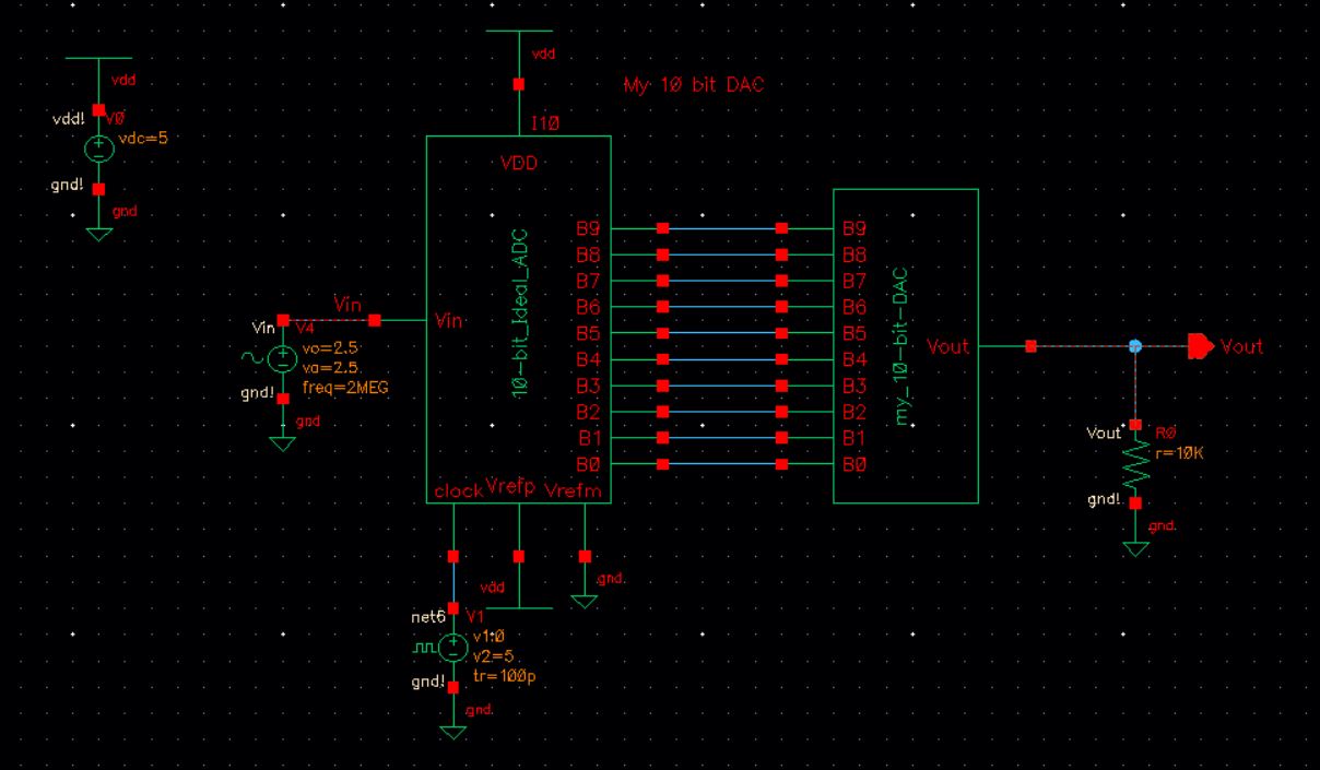
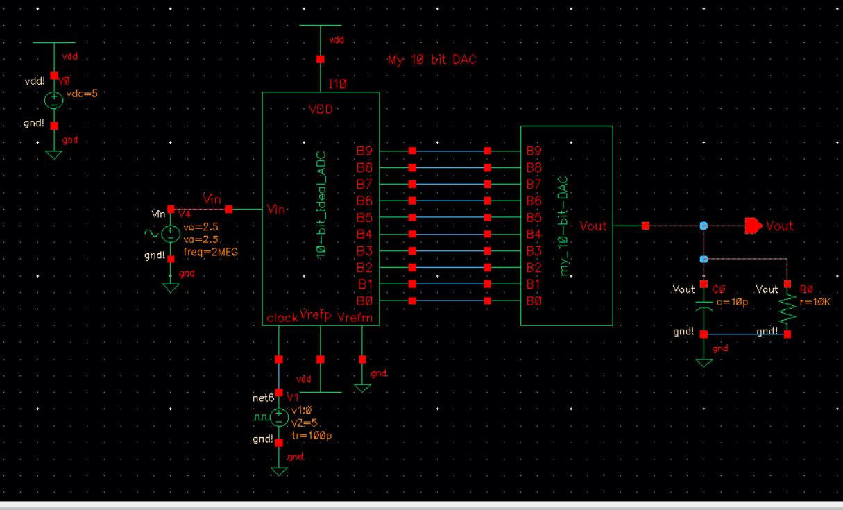
Design of the a 10-bit DAC using an n-well R of 10K
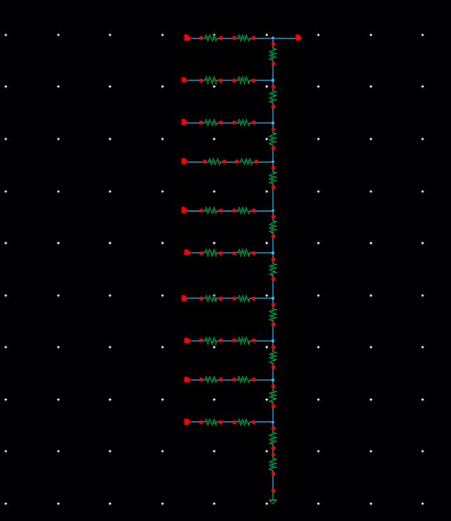
Determining the output resistance of the DAC
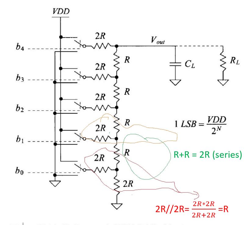
Although
the schematic above shows a 5-bit DAC, the calculations are
similar with a 10-bit DAC. In order to calculate the out put
resistance, we solve the alternating two 2R parallel and two R series
resistors one after the other. Indeed, that results in the total resistance of R.
Delay and driving a load:
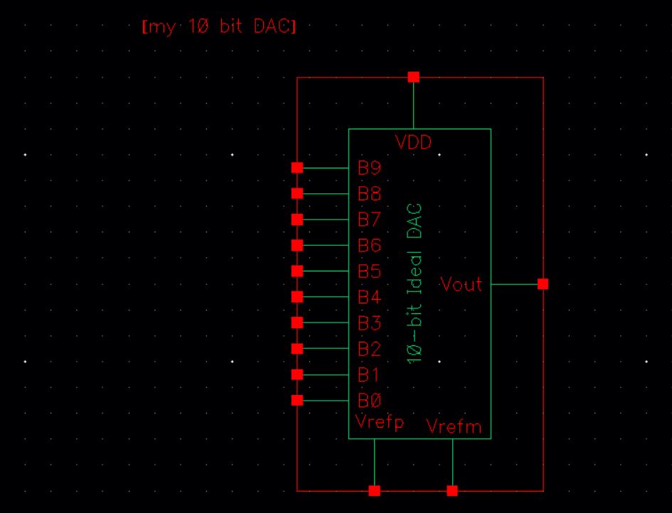
Here
i created the symobol view of my design first before i ground all DAC
inputs except B9 to predict the delay of the DAC having a 10pF load.
Created symbol ( indeeed i deleted Vdd, Verfp, and Verfm pins since my design won't use it.)
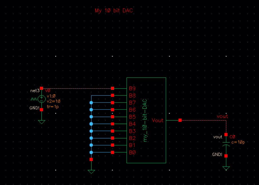
The
schematic( symbol created) with all DAC inputs except B9 grounded,
and B9 connected to a pulse source with 10 pF being driven by the DAC:
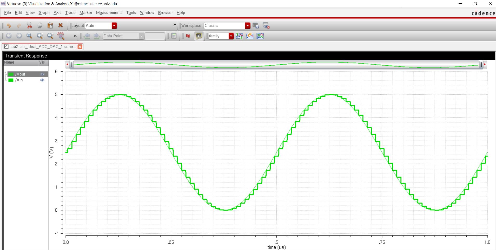
Simulation results:
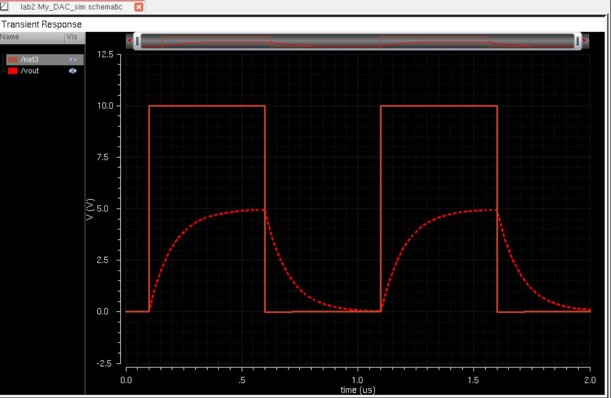
Hand Calculation:
Ʈ = R*C = 10kΩ*10pF = 100ns
0.7RC = 0.7*100ns = 70ns
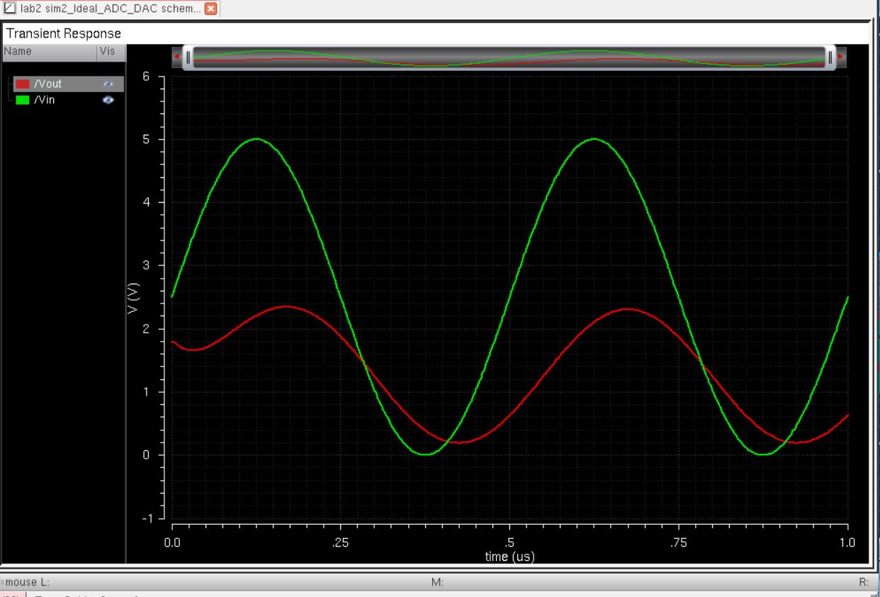
Copying
the Schmeatic cell view sim_Ideal_ADC_DAC to a cell and replacing the
ideal DAC with the one i designed above results in the schematic
attached below.
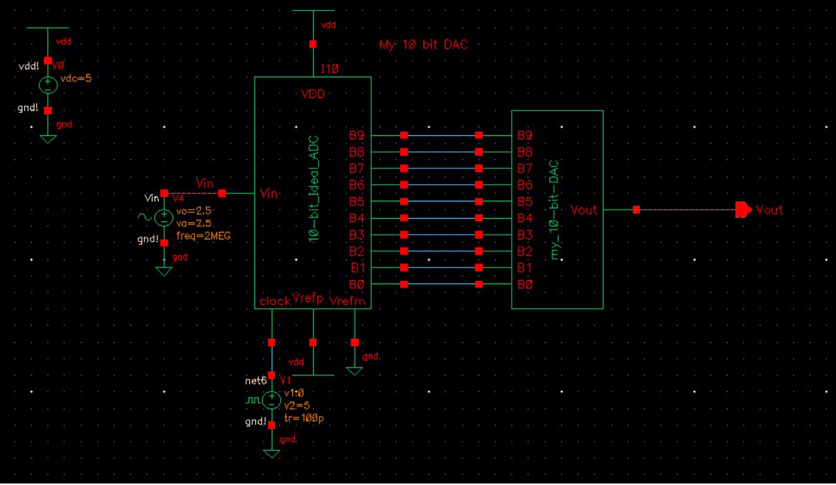
Simulation of the above Schematic:

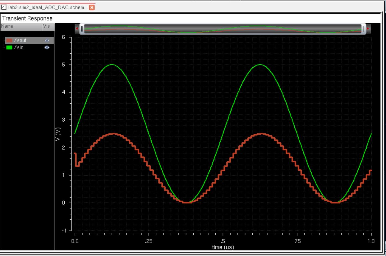
What happens if the DAC drives a 10k load?
If
th DAC drives a 10k load, the output voltage reduces in half because of
a voltage divider it creates and it is demostrated below.
Schmematic of the DAC with a 10k load:
Simulation of the DAC with a 10k load :
Schematics of the DAC with a 10pF Capacitor:
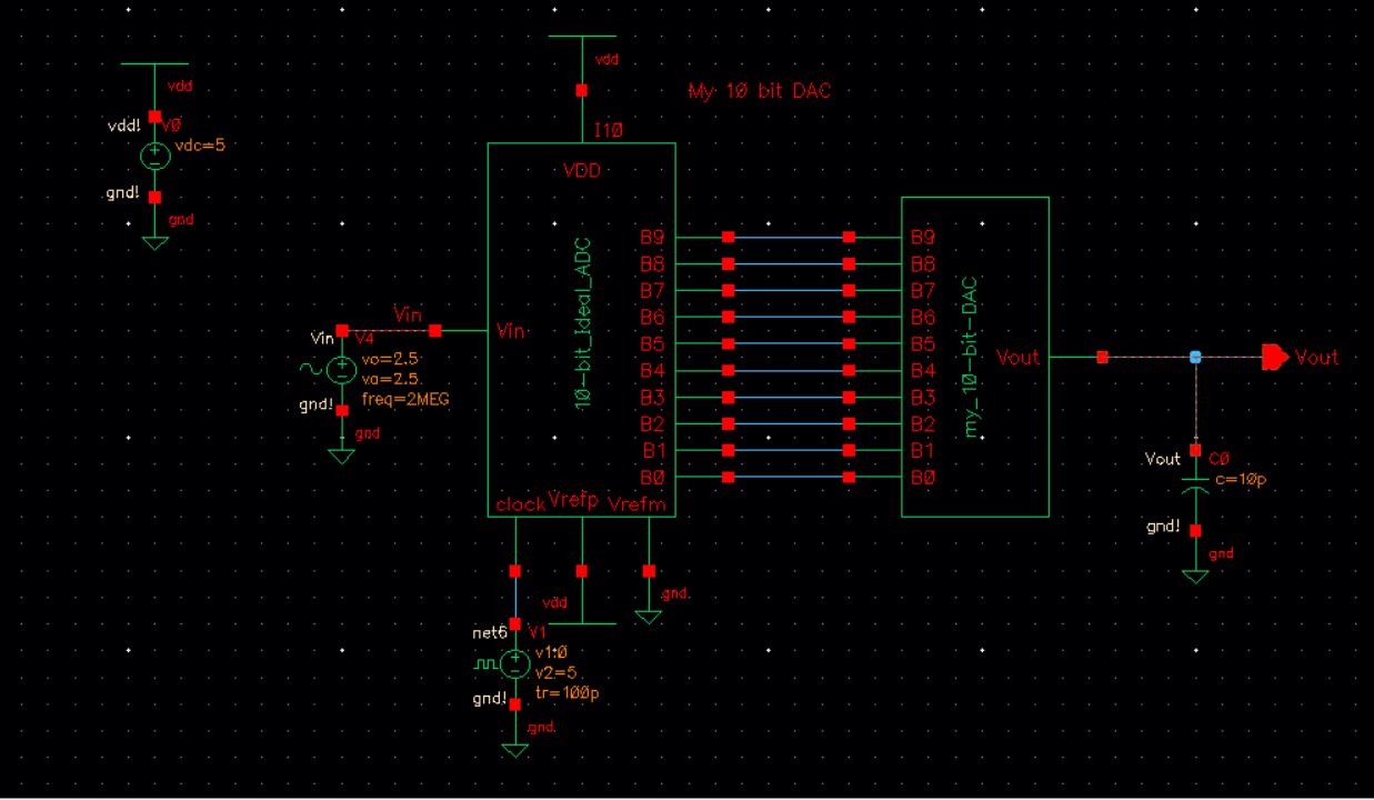
Simulation of the DAC with a 10pF Capacitor:
Schematics of the DAC with both the 10k resistor and 10pF capacitor together:
Simulation of the DAC with both the 10k resistor and 10pF capacitor together:
What happens if the resistance of the switches isn't small compared to R?
If the resistance of the of
the resistor isn't small enough compared to R, it will result in a
reduced voltage in the output because the switch will tend to act as a
resistor when open.
This lab and all pictures and files associated with this lab has been backed up in my drobox.
Return to Biruk's labs
Return to EE421L F18 Student's Directory