Project - EE 421L Serial-to-Parallel Converter
Authored
by Biruk Gebremeskel
Email: gebreb1@unlv.nevada.edu
November 14, 2018
Lab
description:
The purpose of this lab is to design a serial-to-parallel converter
that takes serial input data and an associated clock signal and
generate an 8-bit parallel output(word) and a clock.
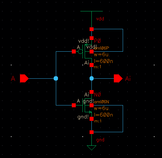
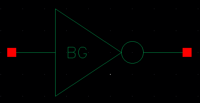
Inverter Schematic and Symbol
Transmission gate(T-gate) Schematic and Symbol
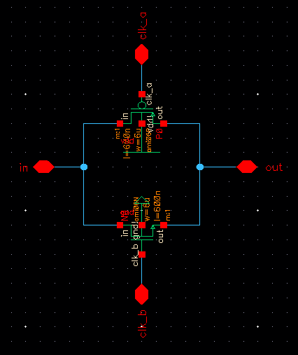
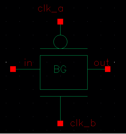
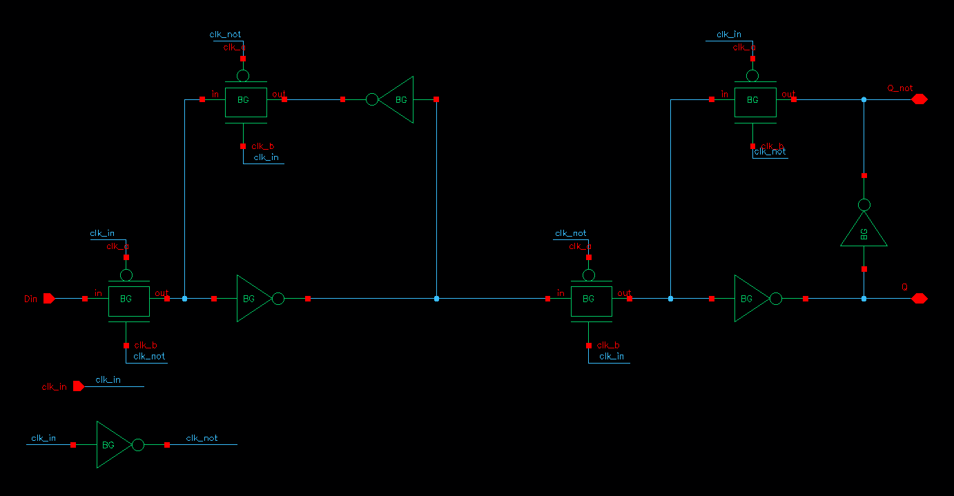
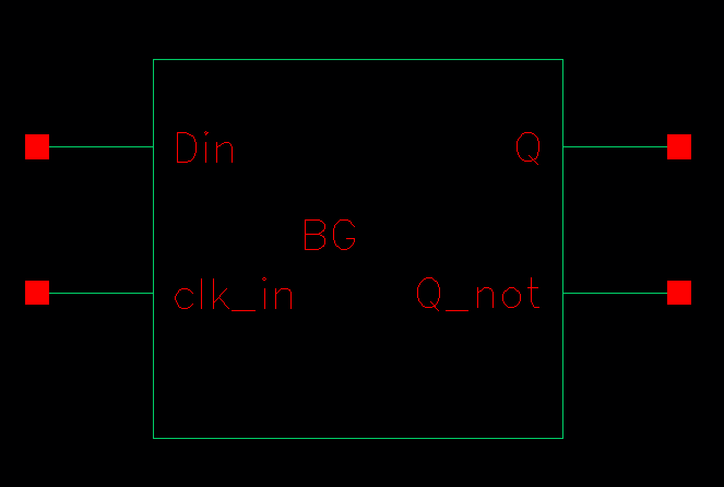
Edge Triggered D-flip flop Schematic and Symbol
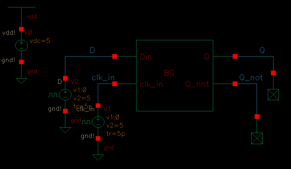
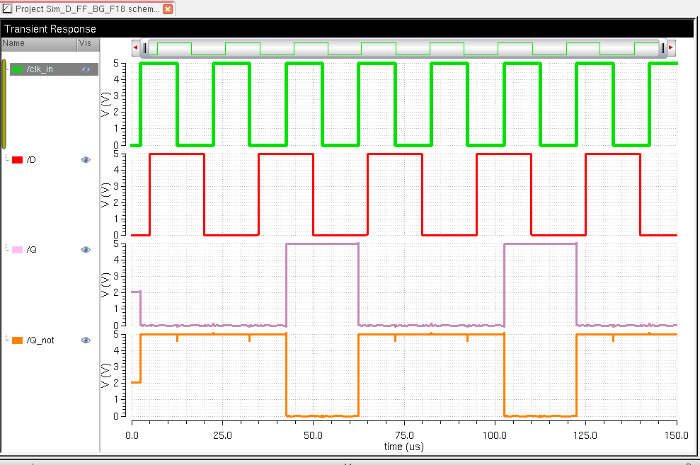
Edge Triggered D-flip flop Simulation
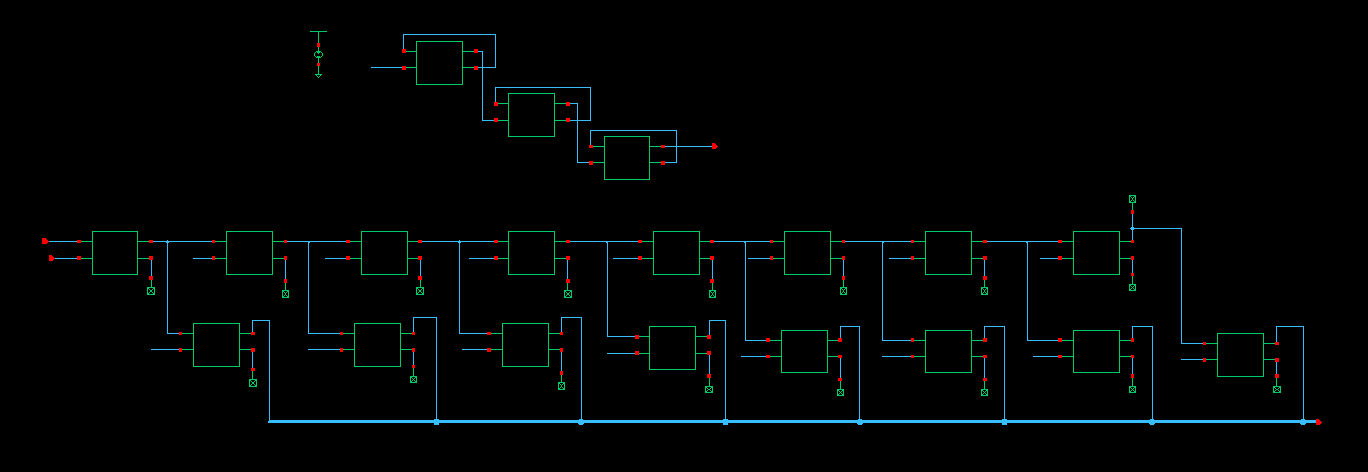
Shift Register Schematic and Simulation
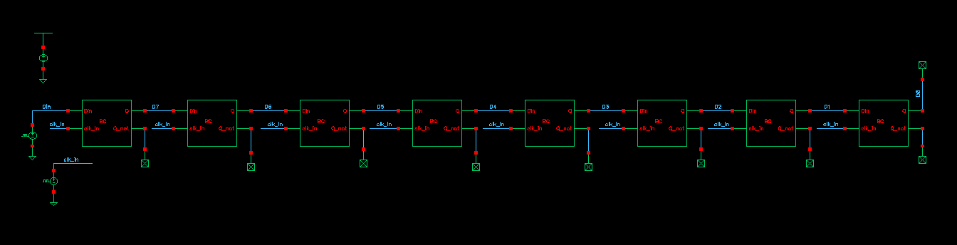
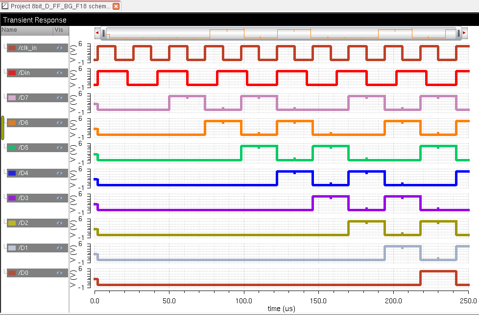
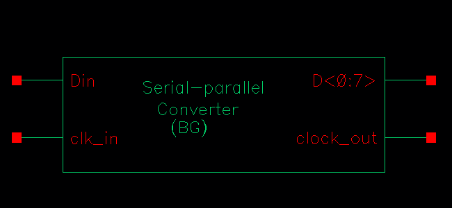
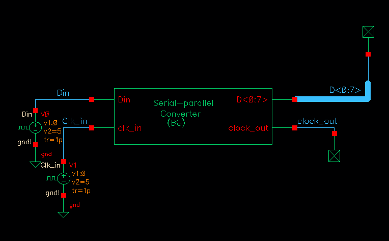
Serial-to-Parallel Converter Schematic, Symbol, and Simulations
 |
 |
 |
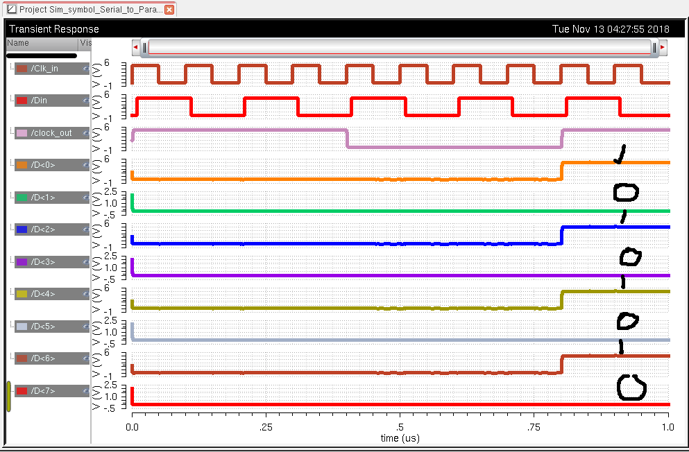
This simulation was tested using the 8-bit binary number 01010101, and it shows in the simulation.
|
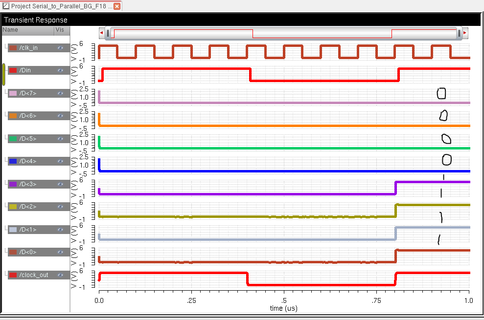
The second simulation is tested using an 8-bit binary number 00001111 as it shows in the simulation.
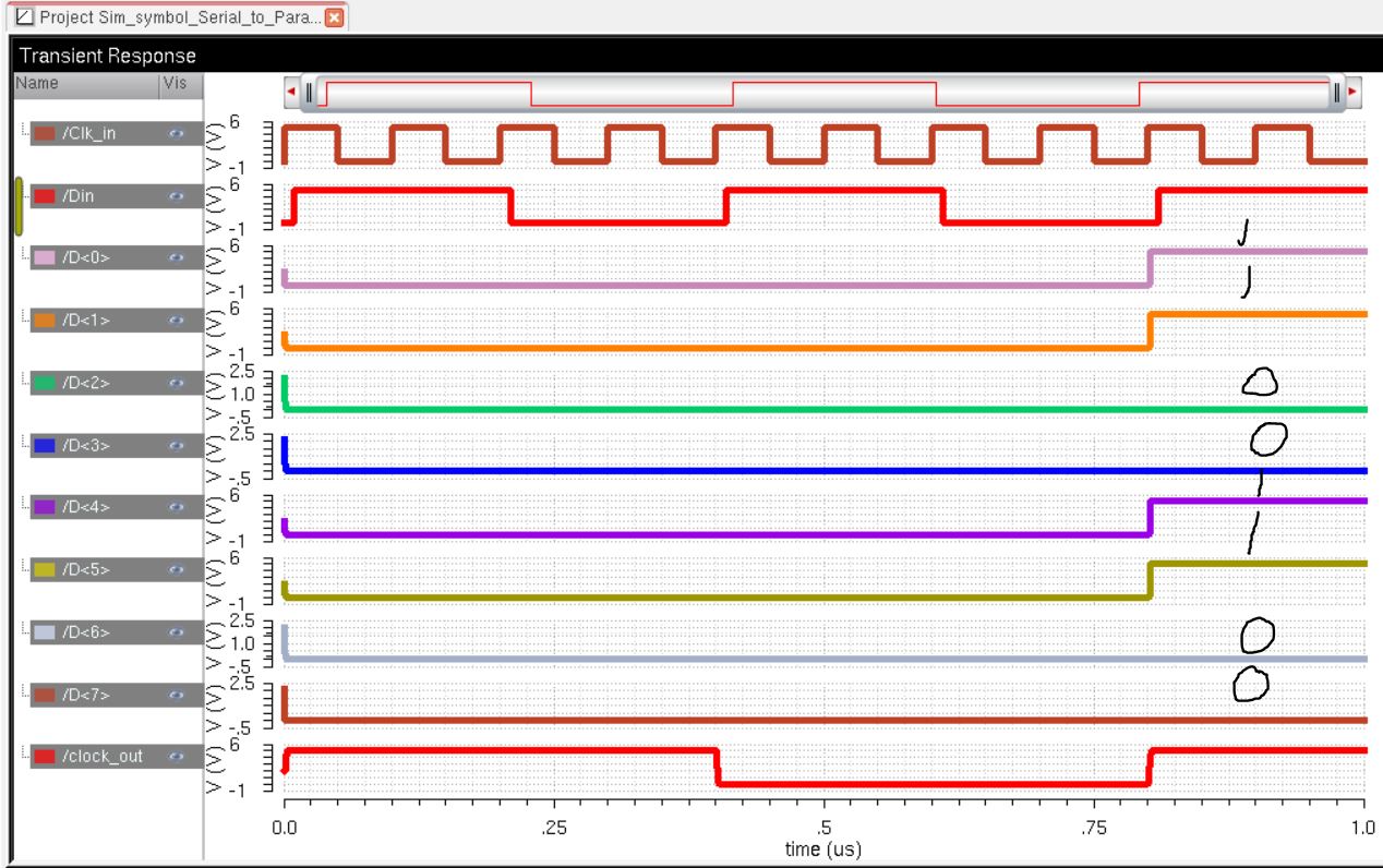
The third simulation is tested using an 8-bit binary number 00110011 as it shows in the simulation below.
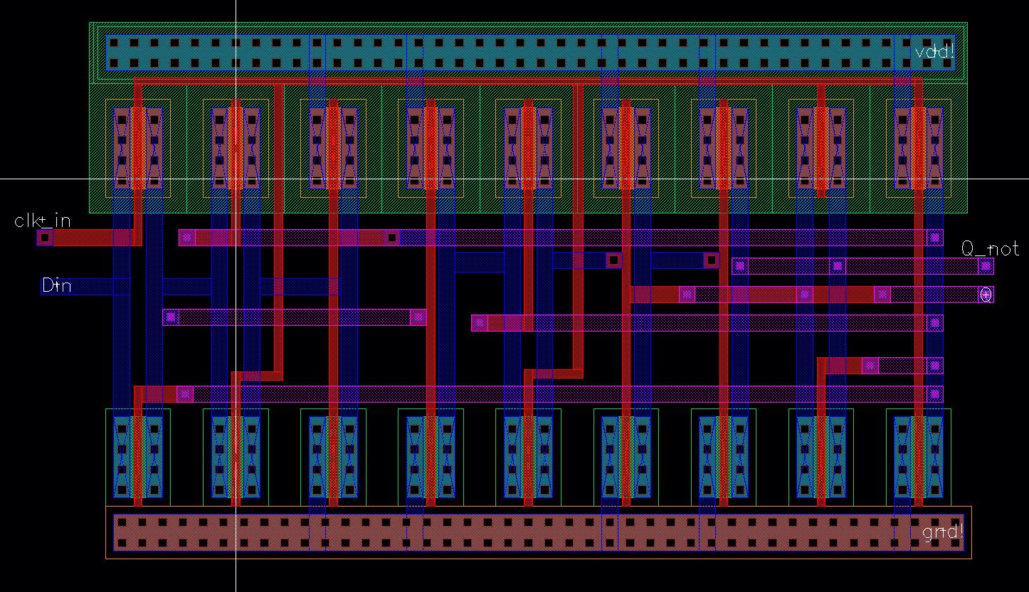
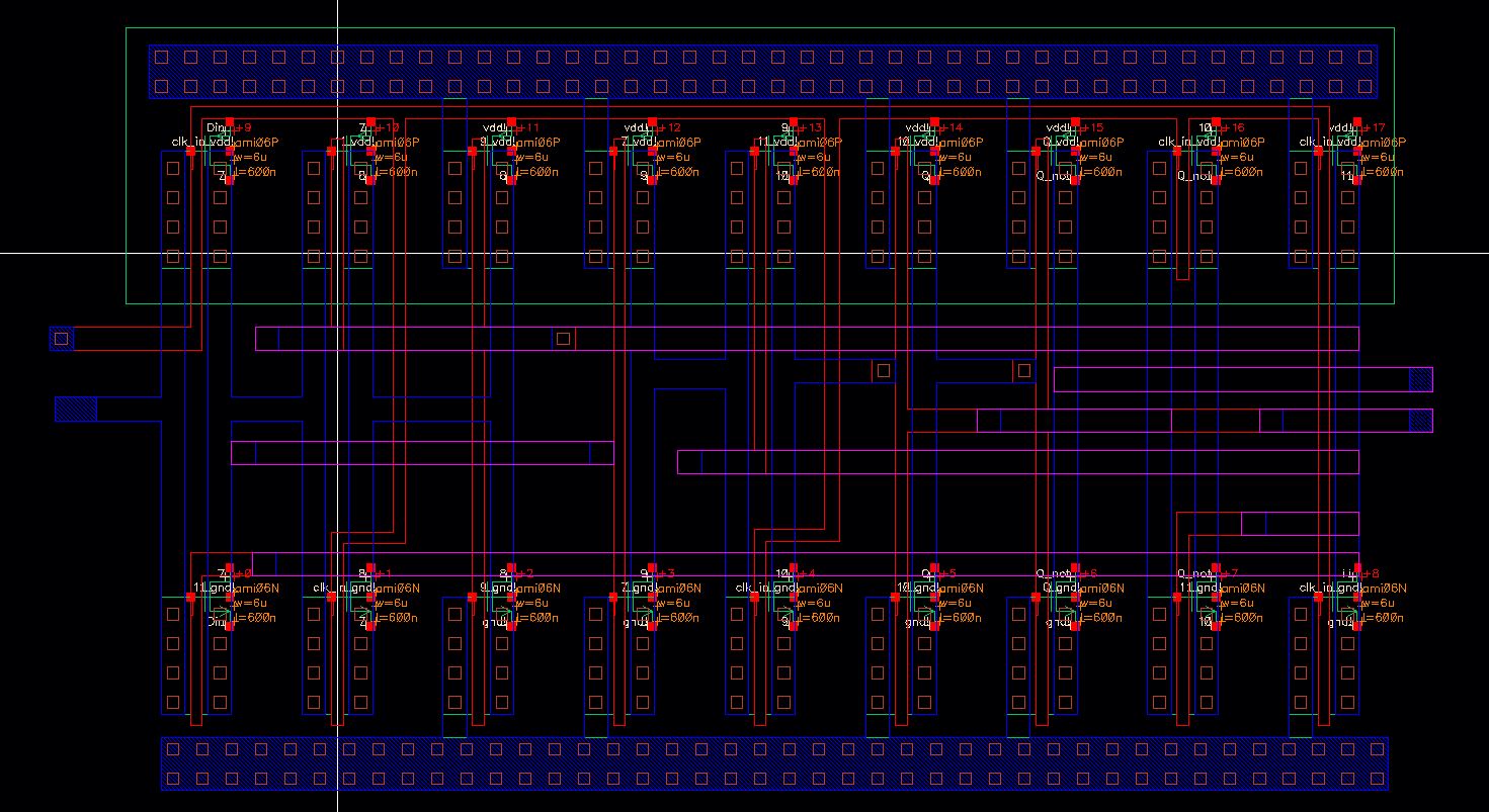
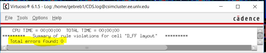
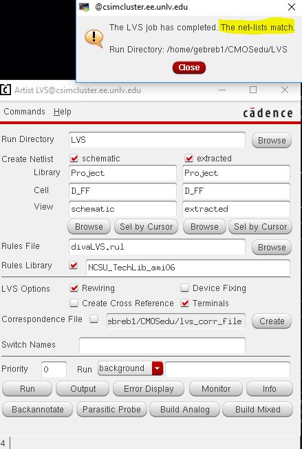
Layout,Extracted, DRC, and LVS of the D-Flip Flop and Serial to parallel Converter
D-FF layout
 |
D-FF Extracted
 |
DRC
 |
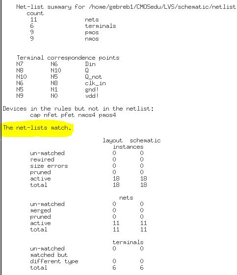
LVS
 |  |
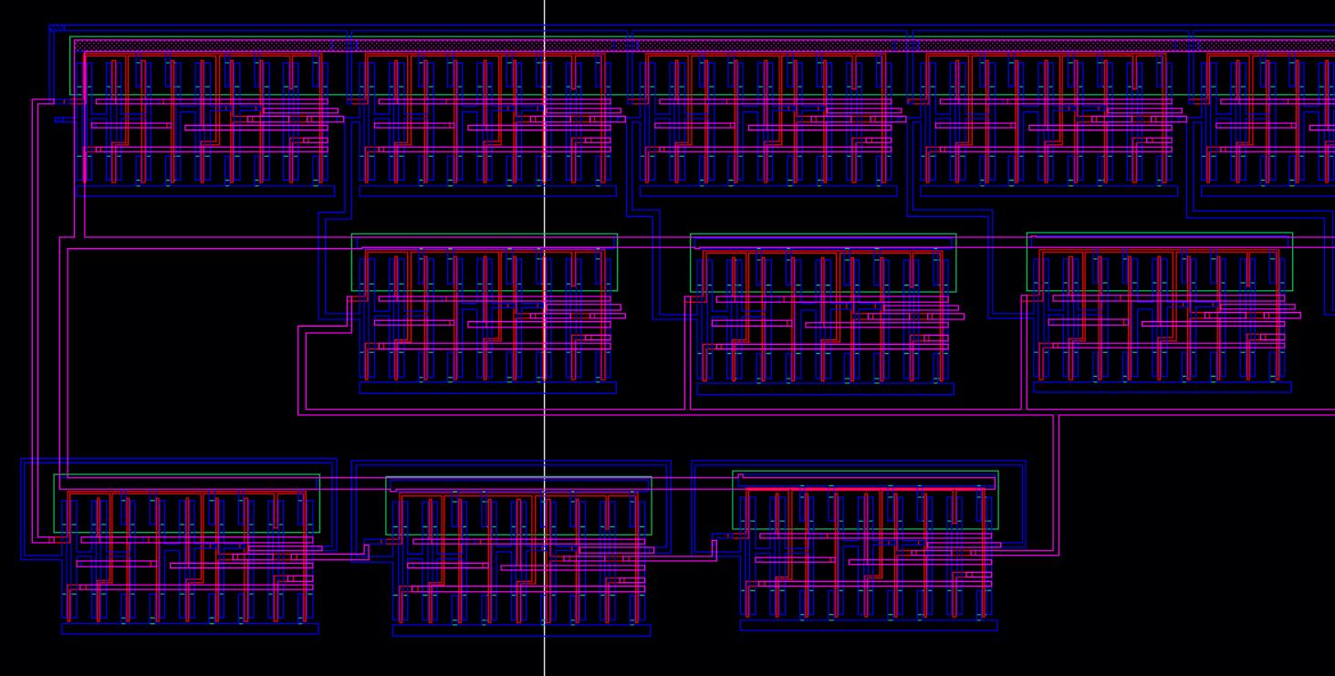
Serial to Parallel Converter Layout
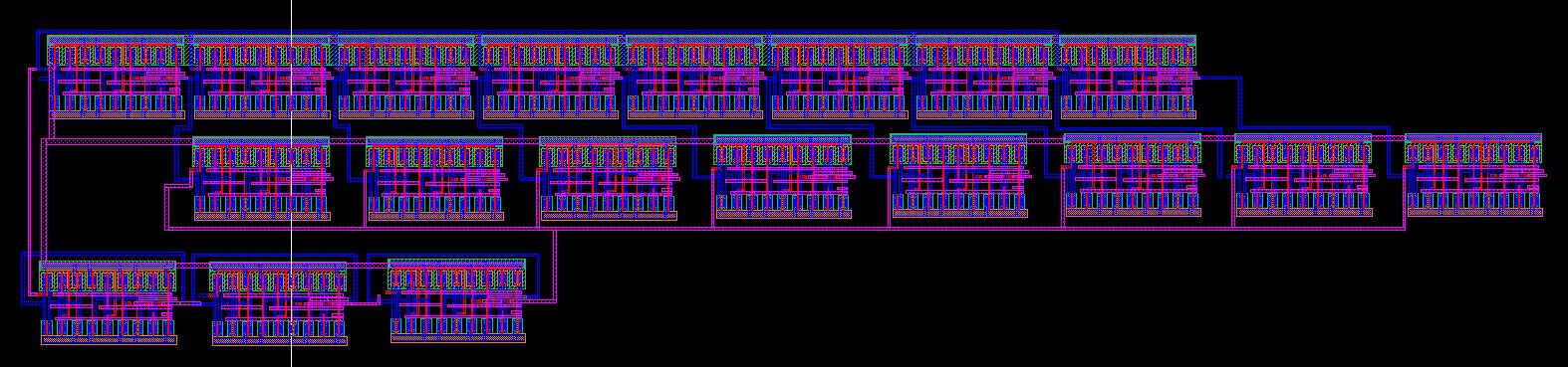 |
Serial to Parallel Converter Extracted
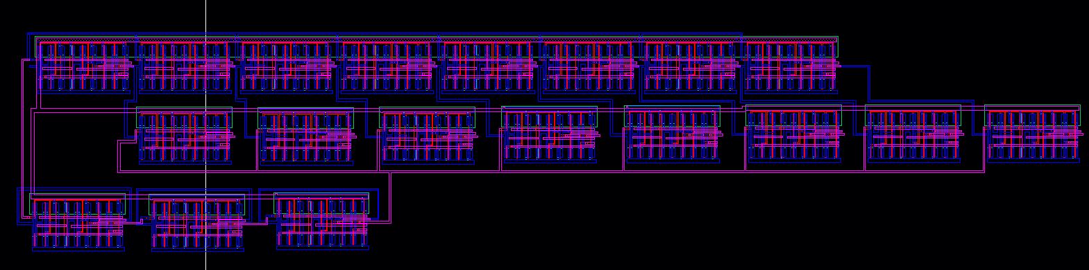 |
Closer but partial views of the layout and Extracted
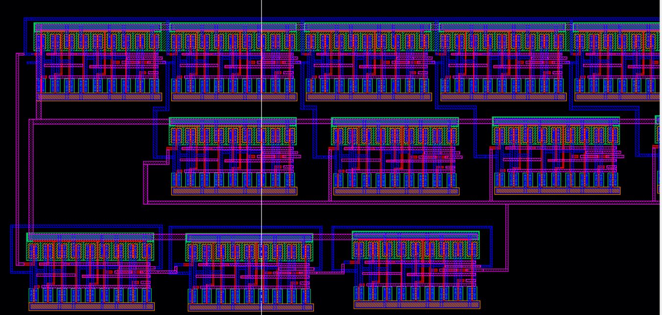 |
 |
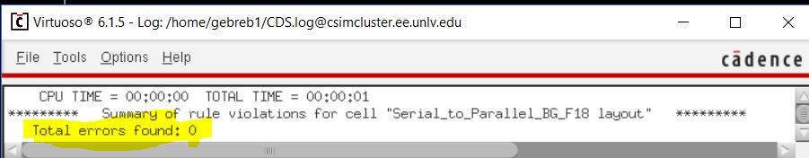
Serial to Parallel Converter DRC
 |
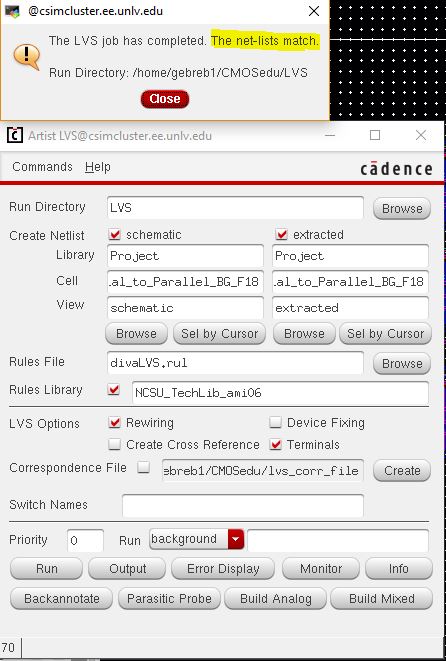
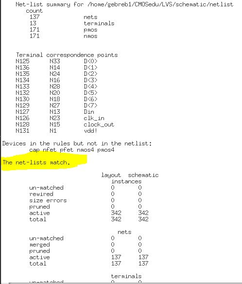
Serial to Parallel Converter LVS
 |  |
All my Cedence schematics, simulations, layouts, etc can be downloaded in the link below.
Proj_BG_F18
Return to Biruk's Labs
Return to EE421L F18 Student's Directory