Lab Project EE 421L – Fall 2018
SERIAL-TO-PARALLEL CONVERTER
Abdals1@unlv.nevada.edu
Files used for
this project project_sa
This project
is the design of a serial-to-parallel converter that takes a serial input
signal and a clock signal and creates an 8-bit parallel word and clock.
Inputs: Din and clock_in.
Outputs: D0-D7 and clock_out.
If the serial
input is 10Mbits/s then the parallel output is 1.25MWords/s.
This project
consists of schematics, simulations and layout.
---------------------------------
PART 1: SCHEMATICS
Transistor sizes: NMOS and PMOS both 6u/600n
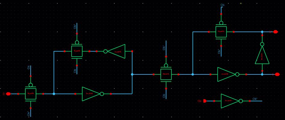
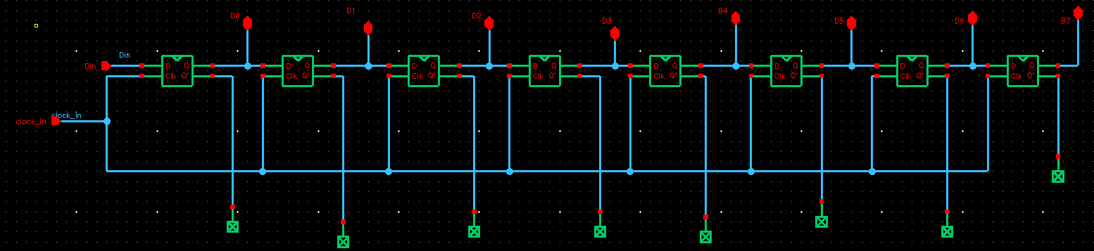
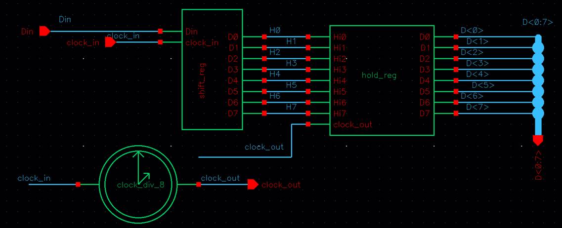
Schematic overview: a serial to parallel converter
is made up of a shift register that reads in a D input value and a clock value,
and a hold register that reads in the output of the shift register as the D
input value and the original clock value divided by eight. Both the shift
register, and the hold register are made up of eight D flip flops. A D flip
flop is created using inverters and transmission gates.
---------------------------------
1.
The first thing I did was create a D-FLIP FLOP using transmission
gates and inverters. To make the design easier to look at, I created individual
cells for the inverter and the transmission gate and made symbols for them.
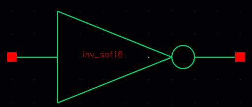
INVERTER SCHEMATIC AND SYMBOL
TRANSMISSION GATE SCHEMATIC AND SYMBOL
D-FLIP FLOP SYMBOL USING TRANSMISSION GATE SYMBOL
AND INVERTER SYMBOL
2.
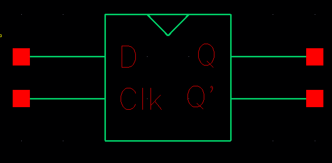
Then I created the D flip flop using the symbols I made
previously. I used Clk and Clk’
as my inputs. I inverted Clk using an inverter. I made
this D flip flop symbol omitting the Clk’ as a pin
because we do not need it after this step. The symbol has a triangle on top to
show that it is edge triggered. The D pin is an input/output pin since we will
be using it as both an input and output since we are cascading D flip flops.
INDIVIDUAL D- FLIP FLOP SIMULATION
3.
I simulated the individual D flip flop first to make sure that it
works. I used two input pulses, D and Clk with values
listed below. I used a shorter delay for the clock because the clock should be
on before D turns on. I did not look at Q’ in this simulation because it’s
result is the inverse of Q. The result of Q shows that the D flip flop works
since it pulses on at the rising edge of clock. The “on” pulse of Q corresponds
to the “on” signal of D at the rising edge of Clk. This shows that the
individual D flip flop works.
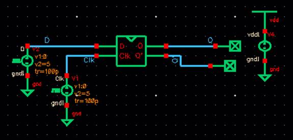
D input
pulse. 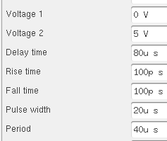 Clock input pulse.
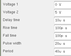
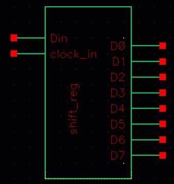
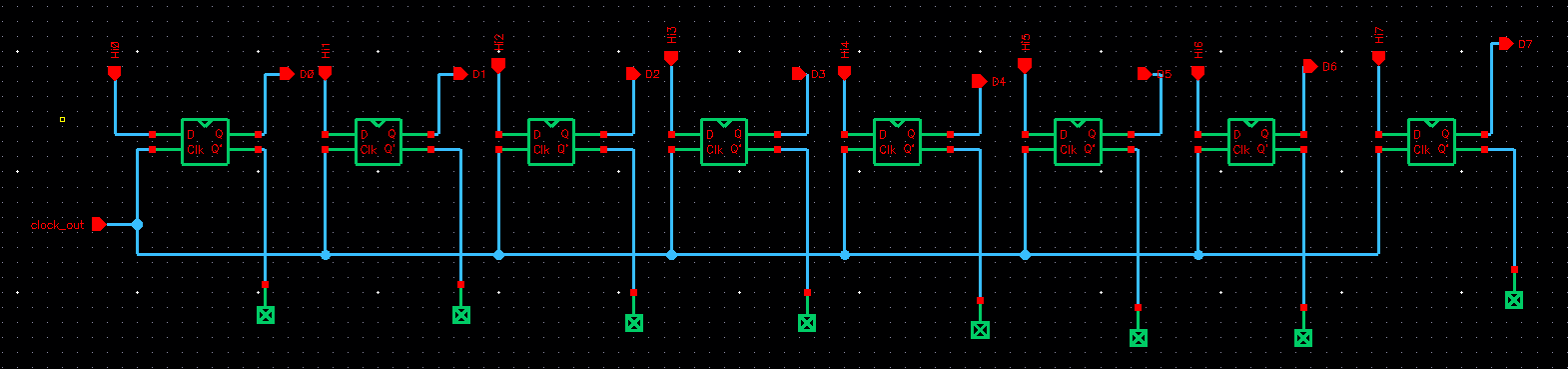
SHIFT REGISTER:
4.
As seen previously, the output of the D flip flop, Q, is the same
as the input D at the rising edge of the clock. In order for
us to create a serial to parallel converter, we need a shift register to move
the data from a serial configuration into an 8-bit configuration as it is
shifted out of the serial input, sequentially. The data input at “Din” is
serial and then is shifted right into the 8-bit shift register. Once the signal
is shifted, it is sent down into the hold register which then shifts it out one
more time to give us our final output. The shift register shown below shows
just the first step: the data is fed in serially and is shifted into 8
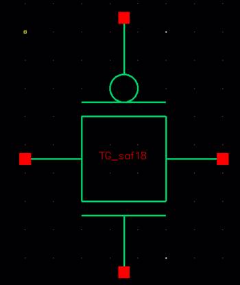
input/outputs: D0-D7. I created a symbol with all 8 input/output pins, the Din:
serial input and the serial clock input.
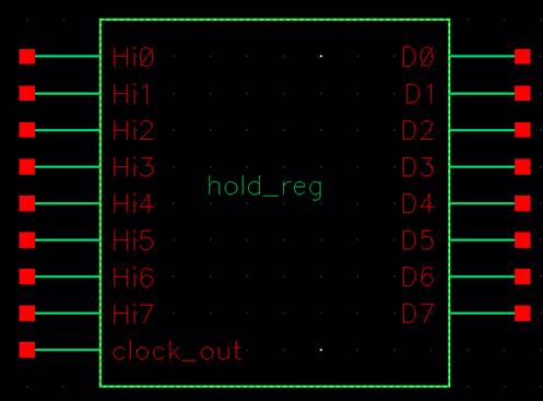
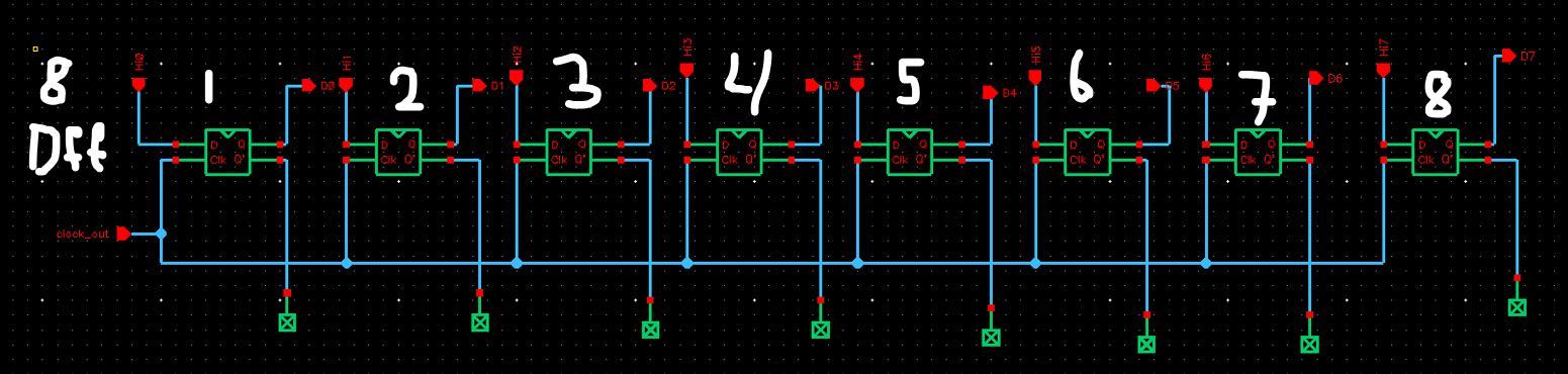
HOLD REGISTER
5.
This hold register is sent the output from the shift register above
into the pins Hi0-Hi8, and sends out the final outputs D0-D7. The outputs D0-D7
are the parallel version of the original input signal “Din”.
The clock that
is fed into the hold register is also the clock/8, or clock_out,
which is the original clock divided by 8.
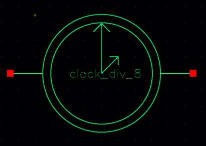
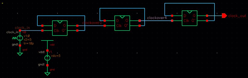
CLOCK/8
6.
This clock converts a 10MHz input into a 5MHz output after going
into the first D-flip flop, then into a 2.5MHz output after going into the
second flip flop, and results as a 1.25MHz output at the final output, clock_out, after entering the third flip flop. I created a
symbol named “clock_div_8” since 10MHz / 8 = 1.25MHz. The output Q outputs
whatever clock feeds in based on the nature of a D flip flop. Then the
inversion of Q is fed back into D. It will output either a 0 or a 1 after the
first D flip flop. The 1 or 0 is just as wide as the entire clock cycle, which
in turn is going to cut the clock cycle in half once it outputs. Before the
signal is sent into the D flip flop, the clock cycle is the length of the
period. After the signal is produced by the D flip flop, the period is doubled,
which halves the initial clocks signal. 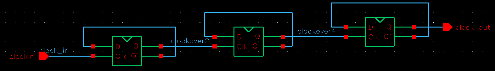
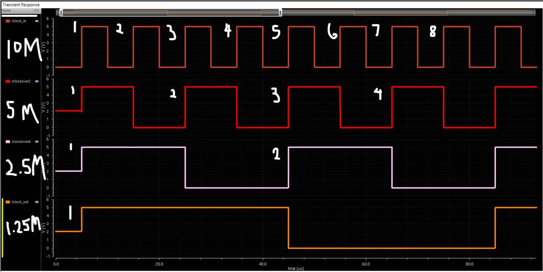
TESTING THE CLOCK
7.
The clock started out as a 10MHz signal with 8 pulses, was divided
by two after the first D flip flop and became a 5MHz signal with 4 pulses, was
divided again after the second D flip flop and became a 2.5MHz signal with two
pulses and finally was sent into the third D flip flop and became a 1.25MHz
signal with one large pulse. The period doubles every time the signal comes out
of a D flip flop.
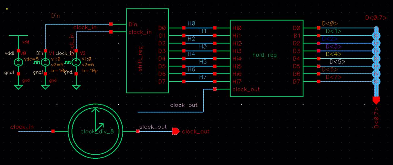
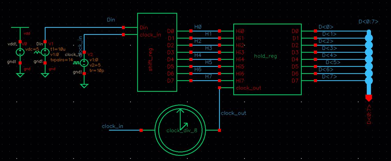
SERIAL TO PARALLEL CONVERTER
I put the
previous pieces together and created the serial to parallel converter. As
discussed previously, the D input and the clock input are fed into the shift
register. The output of the shift register is fed into the hold register. The
clock divided by 8 is also fed into the hold register and the output is D0-D7.
TESTING THE SERIAL TO PARALLEL CONVERTER using
varying input pulses
TEST ONE
8-BIT D-FLIP FLOP SIM using two input pulses.
D input pulse 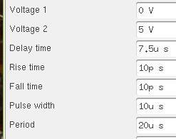 clock input
pulse
clock input
pulse 
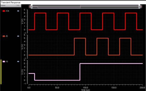
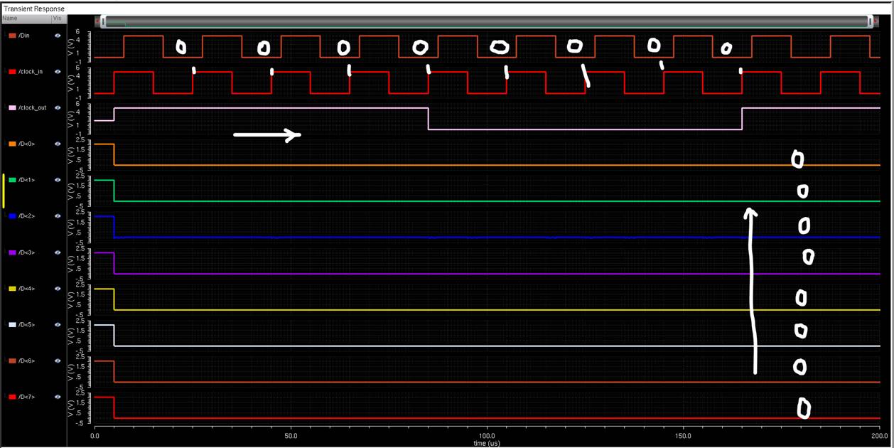
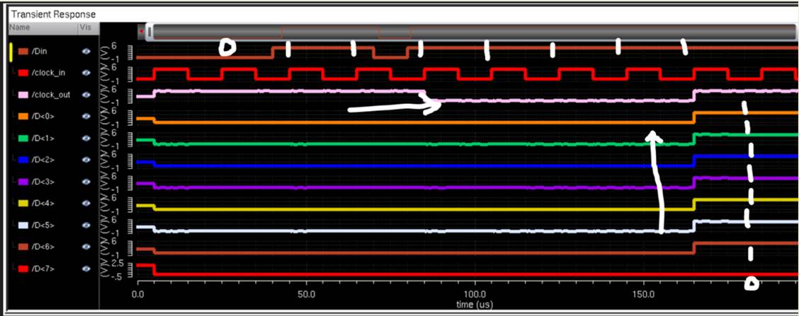
Below you can
see the transient response of the serial to parallel converter. The Serial input
“Din” is above the clock input. We measure the input at the point where the
clock is at the rising edge. I drew a line to show where the clock hits the
Din. I labeled the value of Din at the
clock’s rising edge next to the line. In the response below, the values of Din
were all 0. After the 8th clock cycle, the parallel outputs should
correspond exactly to the serial input.
The output was
00000000. It is read from left to right serially, skipping the first clock
pulse and from bottom to top parallelly.
The
outputs are read from D7-D0.
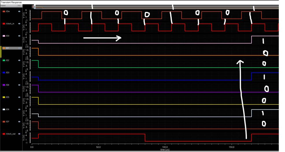
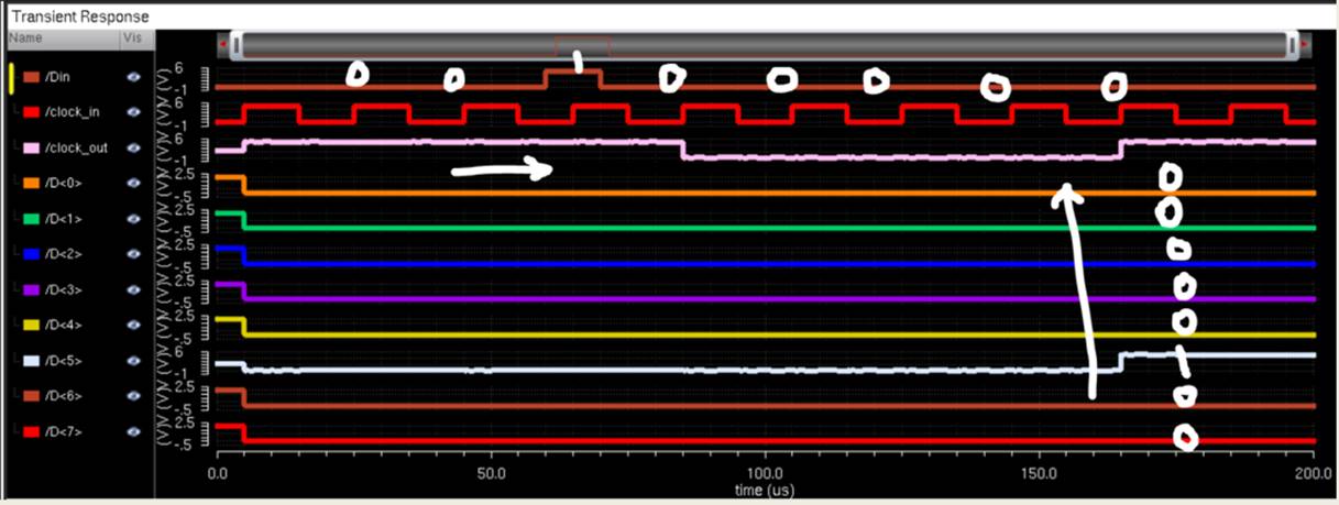
TEST TWO
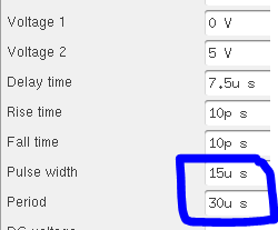
I changed the D
input pulse width and period so that we could get some different input values.
I labeled the values that I inputted serially and put an arrow to show the bit
direction. I also labeled the parallel output with direction to show that my
results correspond to the input.
 I left the clock input pulse the same as it
was previously.
I left the clock input pulse the same as it
was previously.
Just as I did
in the previous example, I measured the input “Din” at the rising edge of the
clock and drew a line to show the correspondence. I also labeled the values of
Din that input serially and the individual outputs that are outputted in
parallel after the 8th clock cycle.
This transient
response outputs 01001001. It is shown from left to right serially, skipping
the first clock pulse, and from bottom to top parallelly. The outputs are read
from D7-D0.
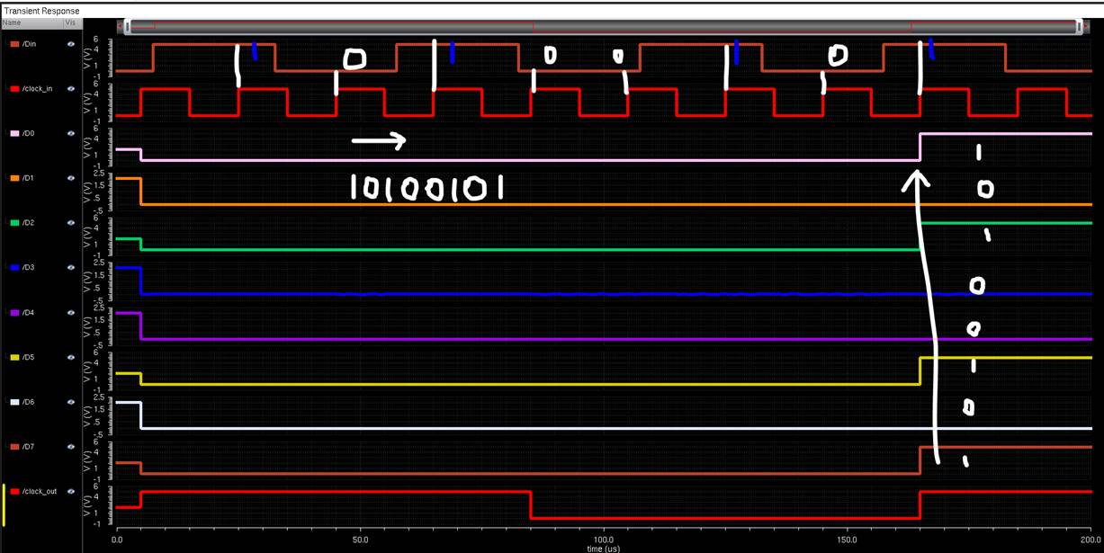
TEST 3
I changed the
Din pulse width to 25u with a period of 50u.
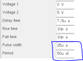 I left the clock pulse at the same rate it
pulsed previously.
I left the clock pulse at the same rate it
pulsed previously.
I measured the
Din at the clock’s rising edge once again, and saw that the serial input
matched the parallel output perfectly.
The output was
10100101. It is read from left to right skipping the first clock pulse,
serially, and from bottom to top parallelly. The outputs are read from D7-D0.
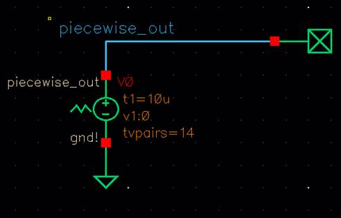
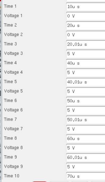
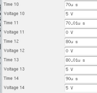
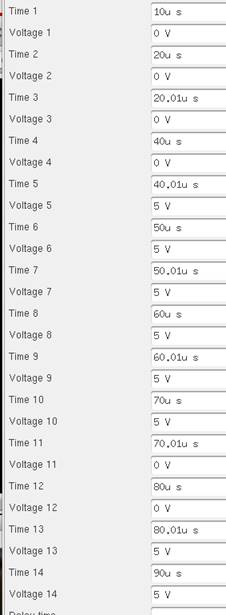
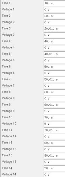
TESTING USING A PIECEWISE LINEAR POWER SUPPLY
I tested the piecewise linear power supply alone first
with the input: 10010101 with a delay of 10u seconds. Every 10u seconds, the
signal changes. The result is shown in the transient response below with
labels.
The output should be 00010101
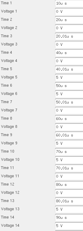
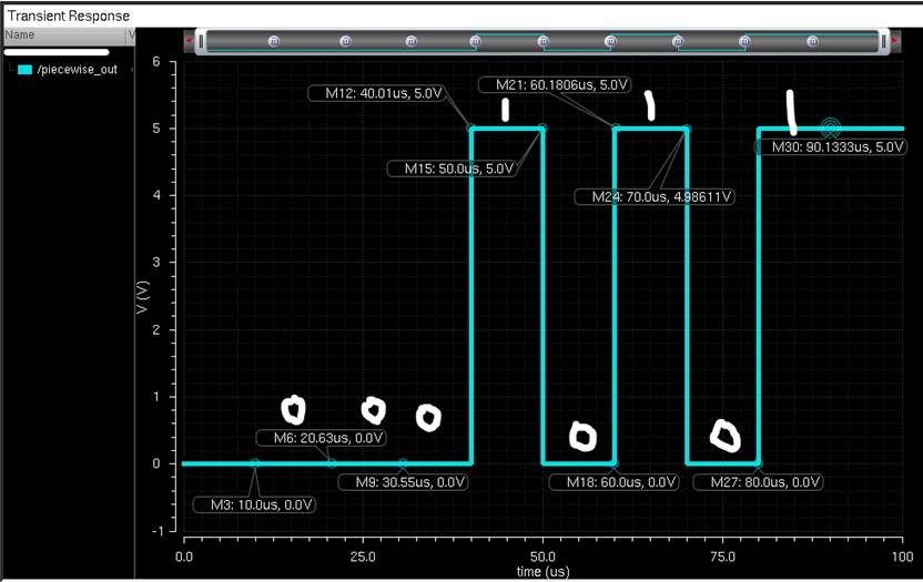
This shows 00010101. The output doesn’t begin
until after 10u seconds. The markers show the change every 10u seconds.
SIMULATING THE SERIAL TO PARALLEL CONVERTER USING
A PIECEWISE LINEAR INPUT “DIN”
TEST 1
I used a different
value of Din. The values I used are below. I left the clock pulse constant for
all of my piecewise linear tests.
The result from reading the D input at the rising
clock edge is 11111111 read from left to right serially and from bottom to top
(D7-D0) parallelly. Both results are the same, which shows that my schematic/
circuit works as intended.
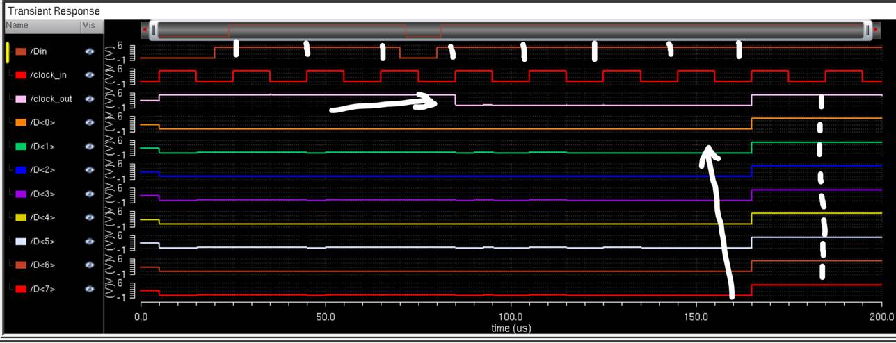
TEST 2
I changed the values in the piecewise linear input
Din.
The value of Din at the rising clock edge is
01111111. The clock input is left at the same value as previously to generate a
consistent test.
TEST 3
I changed the values one more time. The value of Din
is 00100000. The clock is left at the same value, as stated previously.
The
values are read from left to right serially and from bottom to top parallelly.
We can see that the values are the same and the simulation worked as intended.
After testing the circuit six times using two
different methods, it is apparent that the circuit works as intended and converts
an eight-bit serial word input into an eight-bit parallel word output. The
output clock was also successfully divided by eight.
-------------------------------------------------------------------------------------------------------------------------------------------------------------------------
PART 2: LAYOUT
Serial to Parallel Converter layout
The first
thing needed for the serial to parallel converter is the D flip flop. A D flip
flop is made up of transmission gates and inverters.
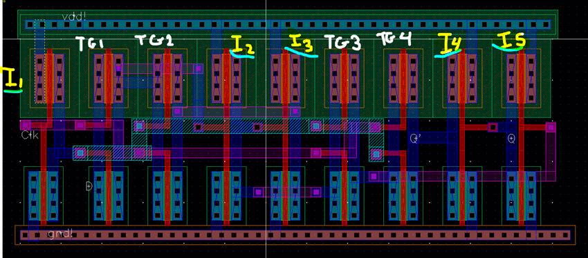
Instead of
laying out the inverters and transmission gates individually and then creating
a D flip flop, I created the layout in one cell instead of instantiating them
in order to create a more cohesive and aesthetically pleasing ntap and ptap connection for vdd and ground. This way, the mosfets
are aligned perfectly and the layout is more concise.
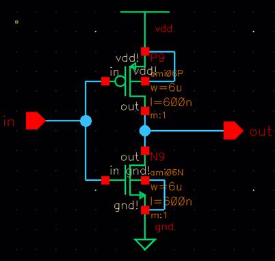
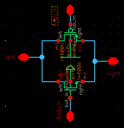
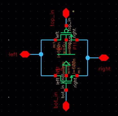
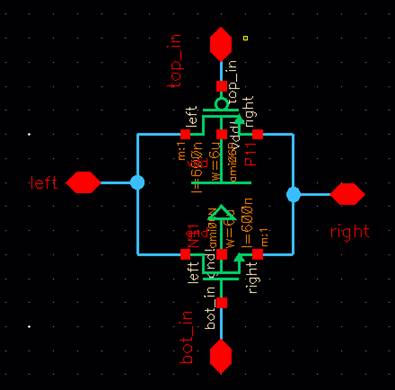
Below is the
inside of the transmission gate. The
sources and drains of the NMOS and the PMOS are connected and the gates hold
different values.
Below is the
inside of the inverter. The source / drain of the NMOS and PMOS are connected,
and the other source/ drain is connected to VDD (PMOS) and gnd
(NMOS). The gates are tied together and the output results from the connected
source/drain.
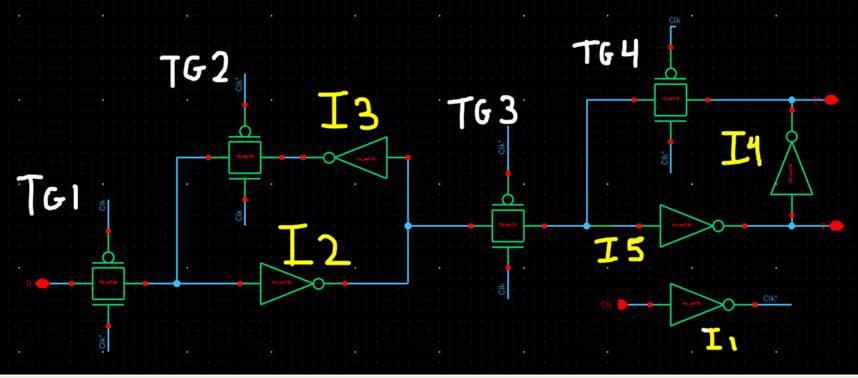
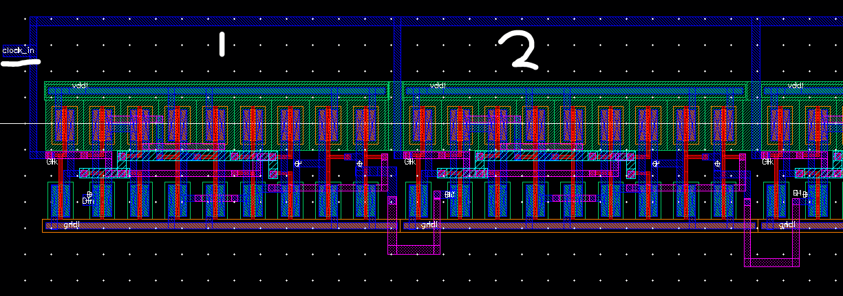
Below is the
layout of the DFF next to the schematic for reference. ‘I’ stands for inverter
and ‘TG’ stands for transmission gate. I labeled the components for easier
viewing.
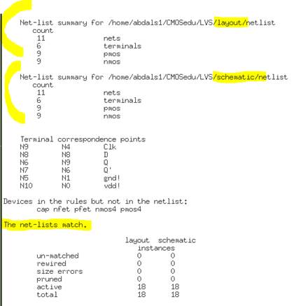
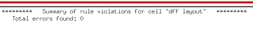
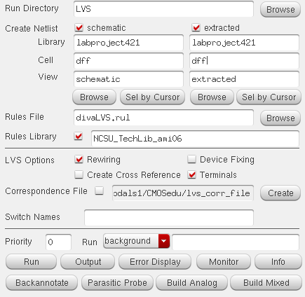
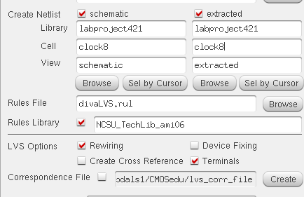
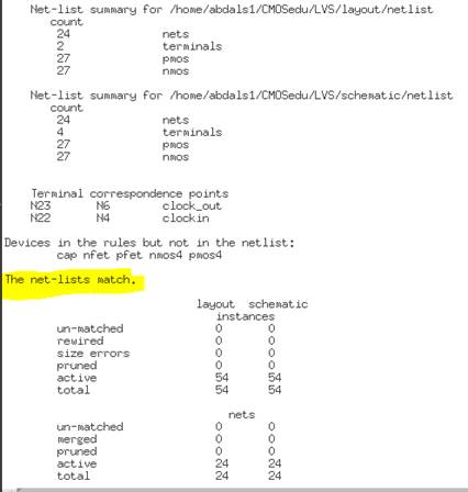
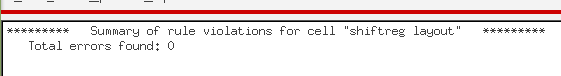
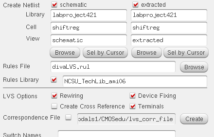
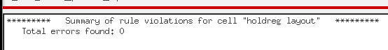
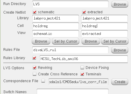
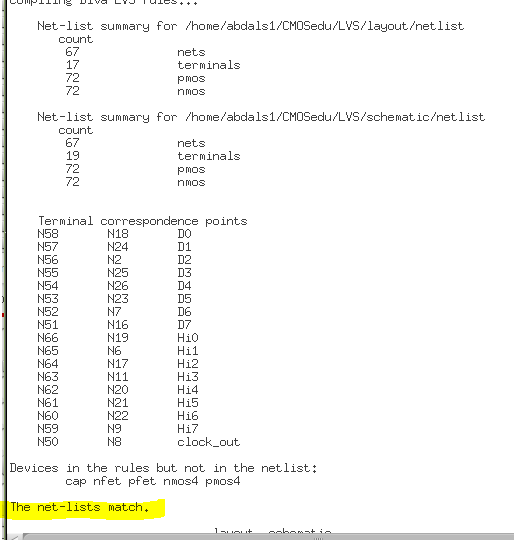
DRC
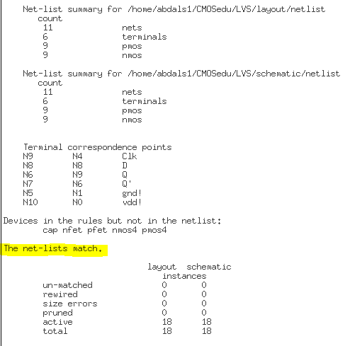
LVS

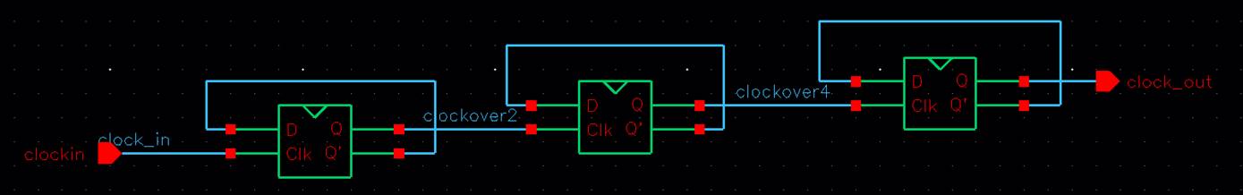
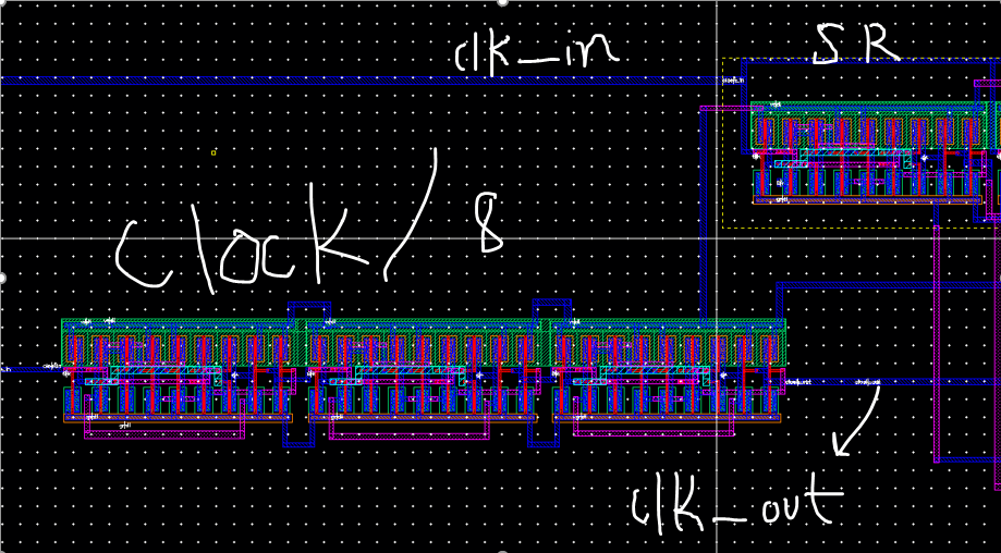
CLOCK/8
Then I used the D flip flop above to create the
clock divider. The input is clockin and the output is
clock_out. The output should be a clock divided by 8.
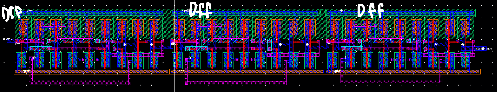
DRC
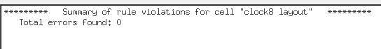
EXTRACTED VIEW
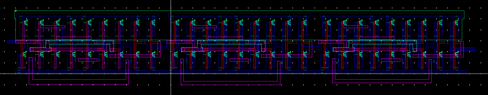
LVS
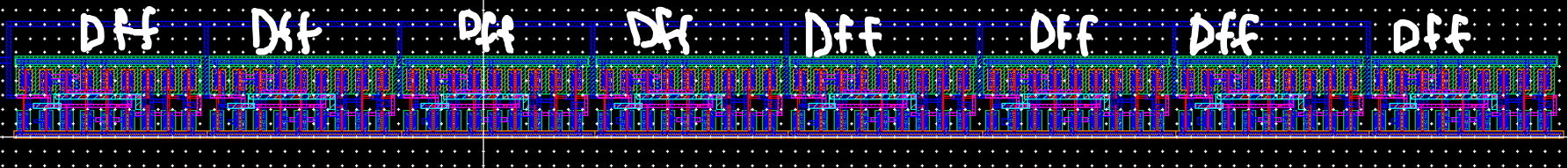
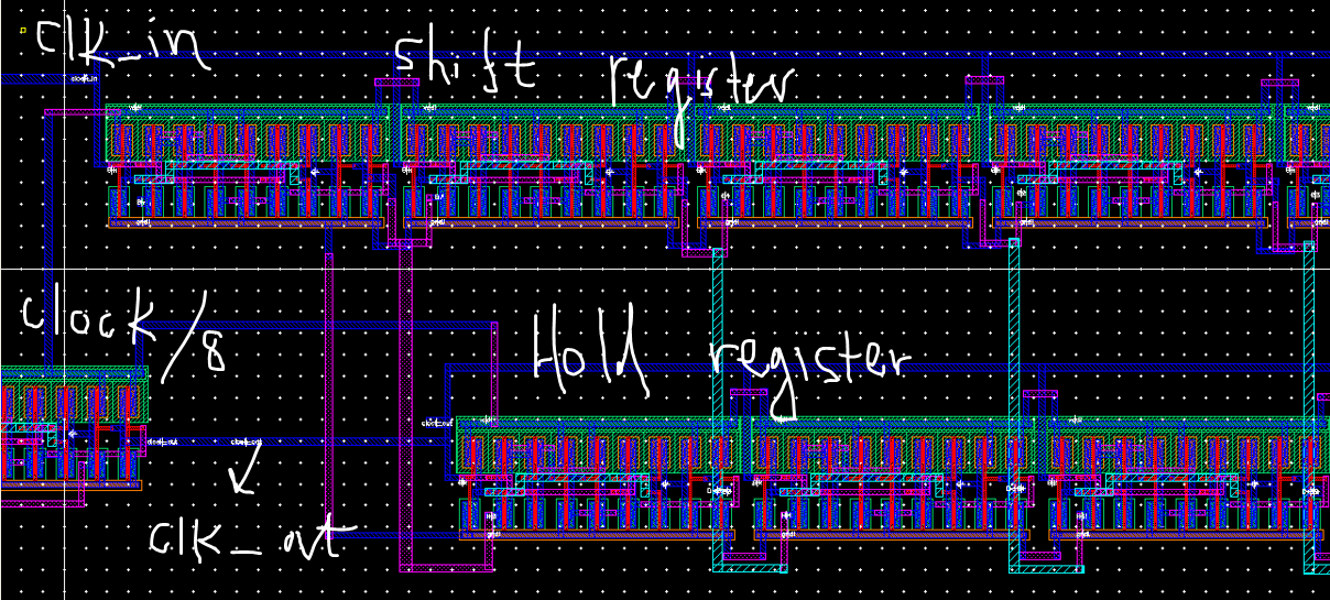
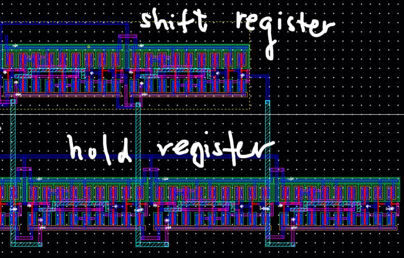
SHIFT
REGISTER
I also used 8 D flip flops to create the shift
register.
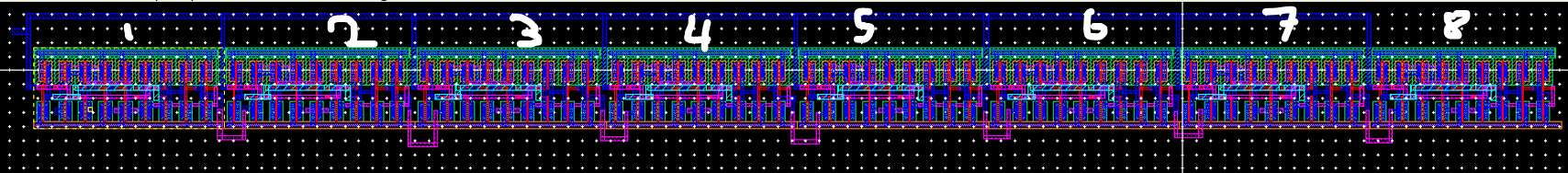
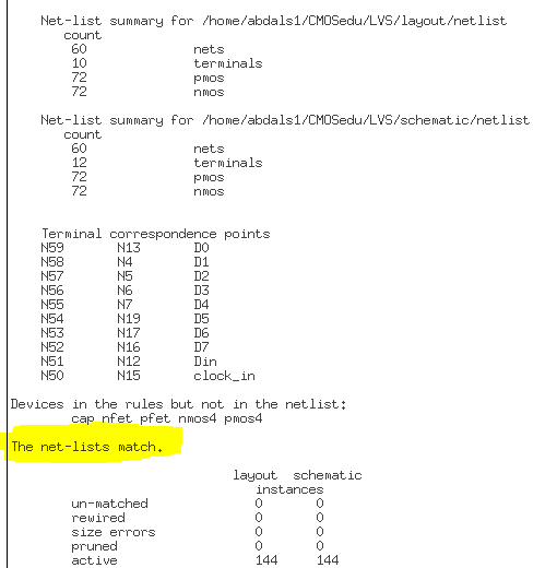
SHIFT REGISTER DRC
EXTRACTED
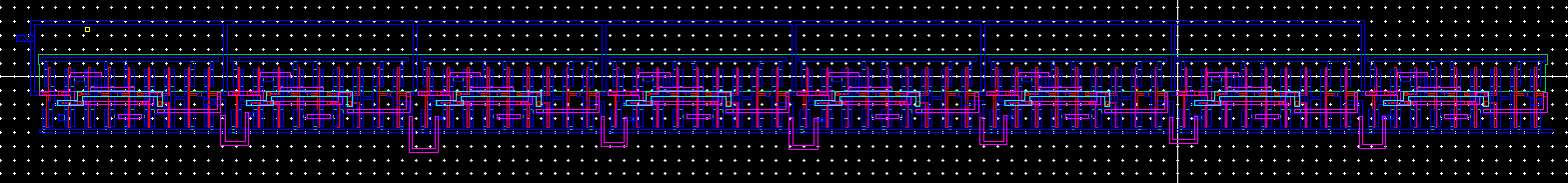
LVS
HOLD
REGISTER:
The hold
register has the input pin “clock_out” which is the
output of the clock divider, the clock divided by 8. The output of the shifter
register is fed into the input of the hold register, Hi0-Hi7. The output of the
hold register D0-D7 is the official output of the entire serial to parallel
converter.
Left side: the clock
here is labeled clock_out because the output of the clock
divider should feed into the hold register, not the original clock input.
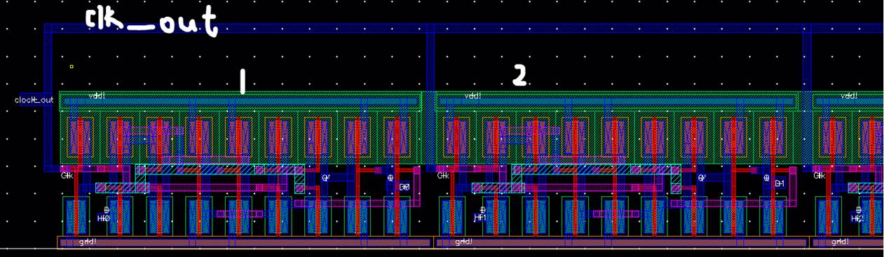
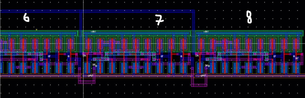
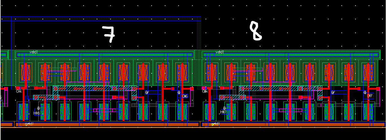
Right side: the 7th and 8th
D flip flops.
DRC
Extracted view

LVS
WHOLE D FLIP
FLOP
SCHEMATIC
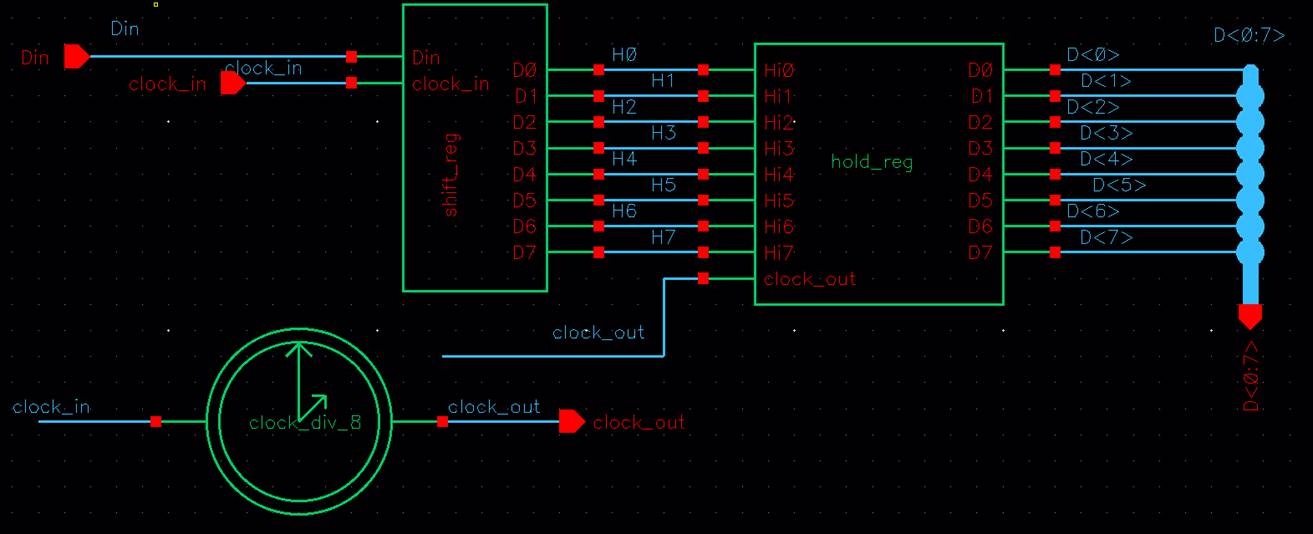
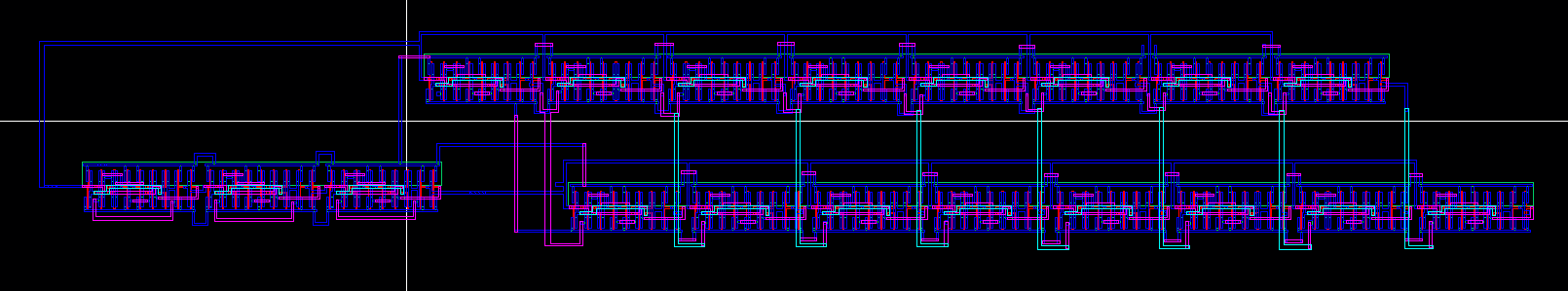
LAYOUT: I connected the clock input to the
shift register’s clock, as well as into the input of the clock divider (clk/8). The output of the clock divider is clock_out which feeds into the hold register. The outputs
of the shift register are inputs to the hold register and the outputs of the
hold register are D<0>- D<7>
which are output pins. Clock_in (input), clock_out (output), vdd!
(input/output), and gnd! (input/output) are some notable
pins that I labeled below.
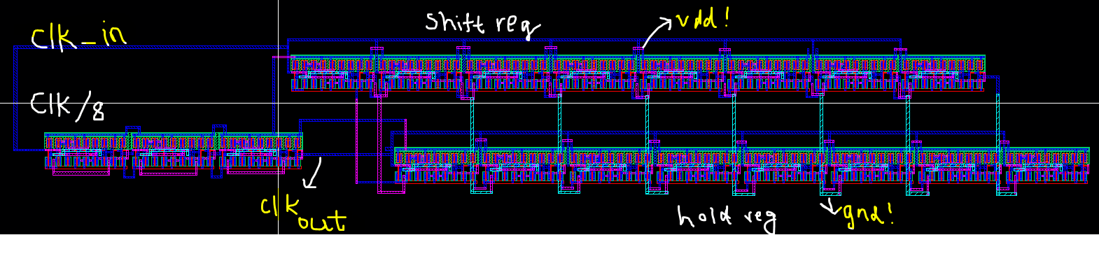
Zoomed in:
Left side: You can see the clock_input
that goes into the shift register and the clock divider. The output of the
clock divider clock_out feeds into the hold register.
Middle connections:
You can see
the clock input feeding into the shift register, and the clock output coming
from the clock divider feeding into the hold register.
Right side:
EXTRACTED
VIEW
LVS