EE 421L Digital Integrated Circuit Design -
Lab 6
Design, layout, and simulation of a CMOS NAND
gate, XOR gate, and Full-Adder
Shadden
Abdalla
In this lab I
will:
1.
Draft the schematics of
a 2-input NAND gate (Fig. 12.1), and a 2-input XOR gate (Fig. 12.18) using
6u/0.6u MOSFETs (both NMOS and PMOS)
2.
Create layout and symbol
views for these gates showing that the cells DRC and LVS without errors
- ensure that your symbol views
are the commonly used symbols (not boxes!) for these gates with your
initials in the middle of the symbol
- ensure all layouts in this
lab use standard cell frames that snap together end-to-end for
routing vdd! and gnd!
- use a standard
cell height taller than you need for these gates so that
it can be used for more complicated layouts in the future
- ensure gate inputs,
outputs, vdd!, and gnd! are all
routed on metal1
3.
Use cell names that
include your initials and the current year/semester, e.g. NAND_jb_f19 (if it
were fall 2019)
4.
Using Spectre simulate the logical operation of the gates for all
4 possible inputs (00, 01, 10, and 11)
- comment on how timing of the
input pulses can cause glitches in the output of a gate
Prelab:
Go through Cadence Tutorial 4. Below is the end
of Tutorial 4.

ACTUAL LAB
- Draft the schematics of a 2-input NAND gate (Fig.
12.1), and a 2-input XOR gate (Fig. 12.18) using 6u/0.6u MOSFETs (both
NMOS and PMOS)
- Create layout and symbol views
for these gates showing that the cells DRC and LVS without errors
- ensure that your symbol views
are the commonly used symbols (not boxes!) for these gates with your
initials in the middle of the symbol
- ensure all layouts in this
lab use standard cell frames that snap together end-to-end for
routing vdd! and gnd!
- use a standard
cell height taller than you need for these gates so that
it can be used for more complicated layouts in the future
- ensure gate inputs,
outputs, vdd!, and gnd! are all
routed on metal1
- Use cell names that include
your initials and the current year/semester, e.g. NAND_jb_f19 (if it were
fall 2019)
- Using Spectre
simulate the logical operation of the gates for all 4 possible inputs
(00, 01, 10, and 11)
- comment on how timing of the
input pulses can cause glitches in the output of a gate
- Your html lab report should
detail each of these efforts
- Below shows (click for a
larger image): 1) schematic of a 2-input NAND gate, 2) schematic of a
2-input XOR gate, 3) simulation schematic, 4) example pulse statement to
generate a digital input, and 5) simulating the operation of the gates
for all 4 possible inputs.
- Using these
gates, draft the schematic of the full adder seen below
- Create
a symbol for this full-adder (example)
- Simulate,
using Spectre, the operation of the
full-adder using this symbol
- Layout the
full-adder by placing the 5 gates end-to-end so that vdd!
and gnd! are routed
- full-adder
inputs and outputs can be on metal2 but not metal3
- The
cells used to generate the images used on this webpage are found in lab6.zip
*********************************************************************
1.
Schematics of a 2 input NAND gate and a 2 input XOR gate using using 6u/0.6u
MOSFETs (both NMOS and PMOS)
NAND
Using
personalized cell view with my initials and year, SA.
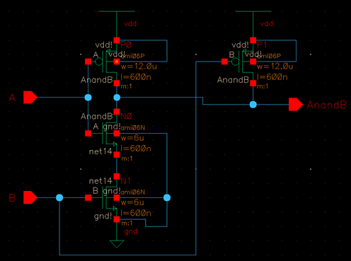
Below is the
NAND circuit using two PMOS’s and two NMOS’s. I used three pins, A and B input
and AnandB output. The PMOSes
are both tied to VDD and the NMOS on the bottom is tied to ground. The BASE of
the PMOS is connected to VDD and the BASE of the NMOS is tied to ground, which
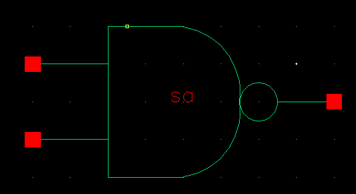
is the general rule. I then created the symbol for the NAND that I created and
put my initials in it.
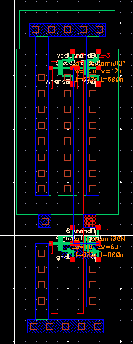
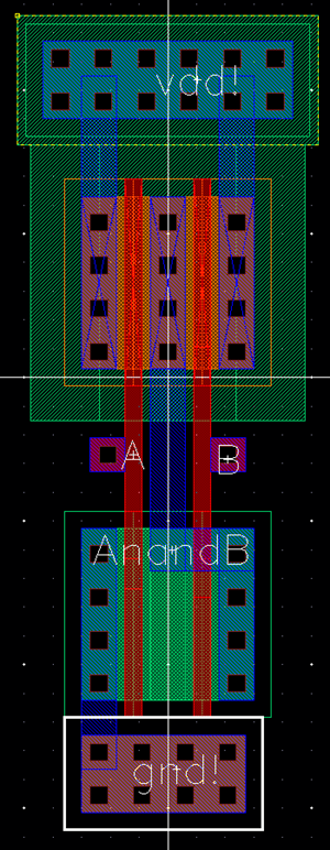
I then created
the layout for the NAND. I used two NMOS and two PMOS just like I did in the
schematic. You can tell that I have two of each MOSFET because of how many POLY
lines there are. In the top PMOS there are two lines of poly, thus there are
two PMOSes there. The bottom NMOS also has two lines
of poly which align with the top poly in the PMOS above. Two lines of poly on
the NMOS shows that there are also two NMOSes. I made
three pins using metal1, A and B as inputs and AnandB
as an output pin. The A and B are on m1_poly and are connected to the poly
because A and B are both tied to the gates of the MOSFETS. AnandB
is connected to the Drain of the PMOS so that is where the pin is located. The
top of the PMOS is connected to an ntap
that is tied to vdd! Using the !
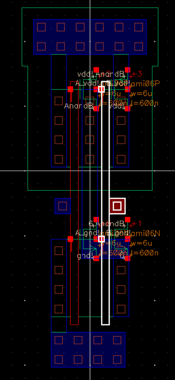
to show the global VDD. The bottom of the NMOS is connected to a ptap which is tied to global ground using the !. I then DRCed and extracted
my layout. After the LVS, you can see that the netlists match.
The DRC of my
NAND layout.

You can see
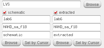
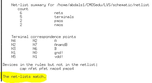
below that I LVSed the schematic and extracted view
and the netlists all matched.
SIMULATING THE NAND
Now, I
simulated the NAND symbol that I created earlier using a pulsing voltage source
from 0 to 5 volts connected to both NAND input terminals so that they can pulse
through all 4 of the outputs asked of us. I tied the output to a 100fF
capacitor. I used spectre to simulate the logical
operation of all 4 possible inputs, 00, 01,10 and 11. I set the VDD value using
the stimuli setting in the ADE. The transient response shows some glitches in
the output when the inputs switch from zero to one or from one to zero.


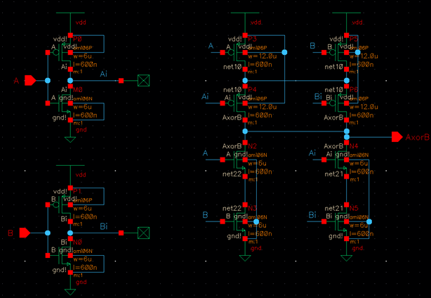
XOR SCHEMATIC AND SYMBOL
I made the XOR
schematic using two inverters on the left holding the values of A and B and put
a noconn unit for the Ai and Bi outputs of the
inverters in order to assign Ai and Bi as well as the
original input pins of A and B into the actual XOR schematic. I used 4 PMOS
devices and 4 NMOS devices. Each PMOS is still connected to VDD a at the source
and the base and each NMOS is connected to gnd at the
drain and the base. The inputs in the XOR are the
actual inputs as well as the inverted inputs. Half of the MOSFETS are connected
to the input pins and the other half are connected to the inverted input. Then
I created the symbol for the XOR with my initials in it.
XOR LAYOUT
I laid out the
XOR using a PMOS and NMOS with four fingers each which represents four mosfets each. Then there are two inverters on the side. The
PMOS is connected to a ntap which has a metal1 pin
connected to vdd! The NMOS is connected to a ptap that has a metal1 pin on it connected to gnd! The A pin is connected to the two gates of the inverter,
the gate of the NMOS and the PMOS. The B pin is also connected to the gates of
the second inverter (gates are on poly), the gates of the NMOS and PMOS. I also
connected the PMOS and NMOSes in the inverter
together using metal 1. The output pin, AxorB
connects the NMOS drain and the PMOS drain.
Then I extracted
the layout.
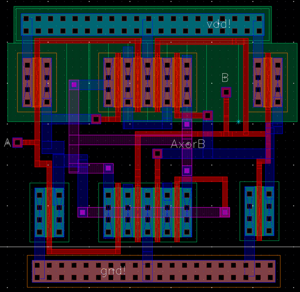
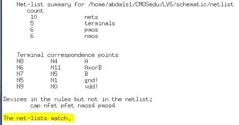
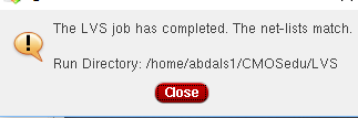
I then DRCed the layout of the XOR.

Then I LVSed the schematic and extracted.
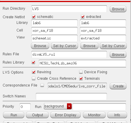
The netlists
matched and the LVS job completed.
USING THE SYMBOLS WE JUST
MADE TO MAKE A FULL ADDER SCHEMATIC
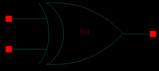
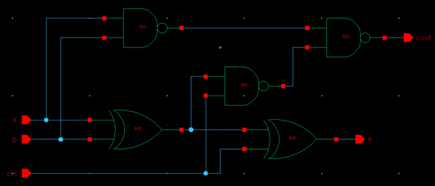
I put together
3 NANDs and two XORs using 3 input pins and two output pins to make the full
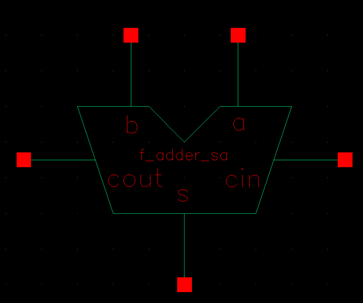
adder, then I created a symbol for it. I used input pins a,b, and cin. I used output
pins cout and s.
To the right
is the chart that gives us what the output and inputs should be for a full
adder.

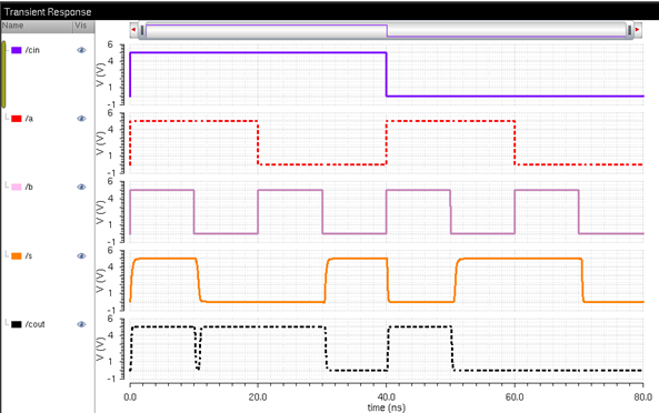
SIMULATION
I simulated the
symbol using the same method as before, three pulsing voltage sources to test
out all three bits. The VDD is also set up using the stimuli setting in the ADE
L.
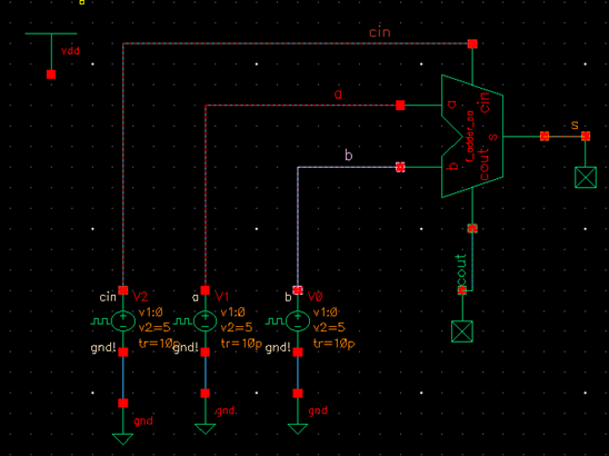
The simulation
showed the same results as the chart.
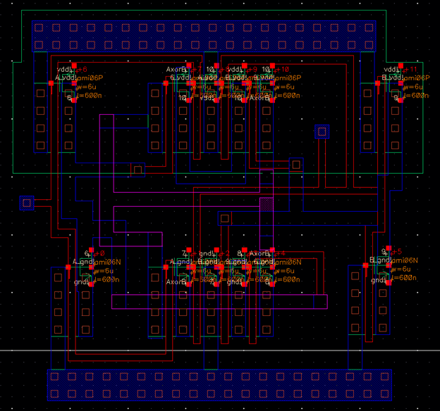
FULL ADDER LAYOUT
I combined all of the previous layouts that I made to make the entire
full adder. I alternated my placement of the NANDs and XORs. I used the same pins
as in the schematic, a, b, cin, s and cout.
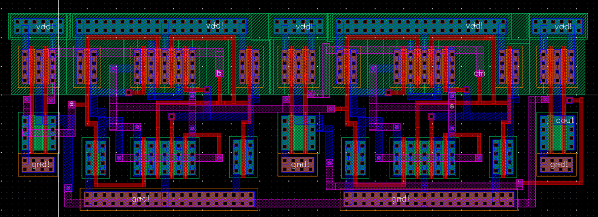
I then
extracted the layout to prepare for LVS.
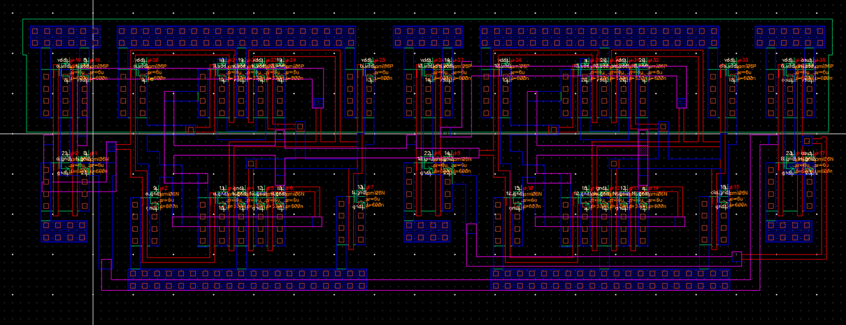
I DRCed the layout and there were no errors.

I LVSed the schematic and the extracted layout and saw that
the netlists matched.


