EE 421L Digital Integrated Circuit Design -
Lab 5
Design, layout, and simulation of a CMOS
inverter
Shadden
Abdalla
September 20,
2019
PRELAB:
Finish tutorial 3.


Above marks the end of tutorial 3.
About this lab
This lab has 3 parts:
Part 1. Draft two
schematics of two different inverters, a 12u/6u and a 48u/24u inverter and the
create symbols for each.
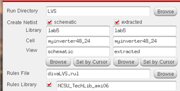
Part 2. Create layout
for both of those inverters, DRC, LVS them versus the schematics created
earlier.
Part 3. Create
schematics using the previously made inverter symbols and simulate them over
four different capacitor values.
Part
1: Inverter Schematics and Symbols
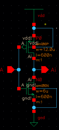
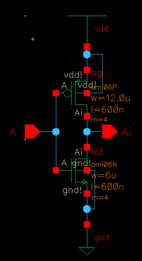
The left schematic is of
an inverter using pmos4 and nmos 4, each as a
multiple of one. The right schematic is of an inverter also using the same
components but instead of just a multiple of one they are of multiple four.
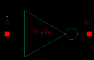
This is the symbol view
that I created for inverter of multiple one (m=1).
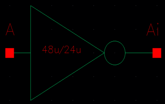
Below is the symbol view
I created for inverter of multiple four (m=4).
Part
2: Inverter Layout and LVS
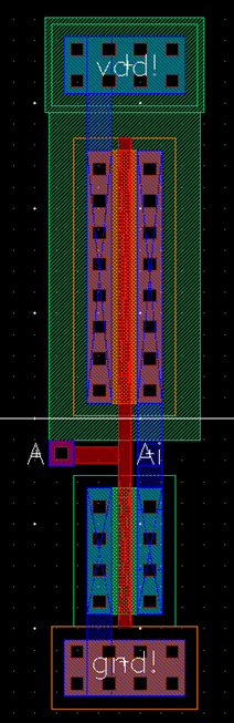
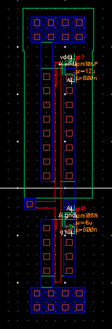
Below are the layout and
the extracted view of the layout for the inverter of multiple one.
The layout shows the
PMOS connected to an ntap
with a vdd! Pin using metal1. Then the nmos on the bottom is connected to a ptap
with a gnd! Pin using metal1. The input A that goes
into the gate is connected to poly which is what connects to the gates. The
output pin is connected to the Drains of the NMOS and PMOS.
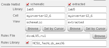
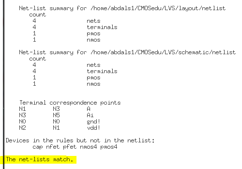
I DRC ed the layout and it had no errors.

I LVS’d
the schematic view of the inverter of multiple one versus the extracted view of
the layout and saw that the net-lists matched, showing that my design was
accurate.

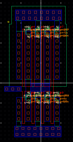
Below is the layout and extracted view of the
inverter of multiple four. I connected the PMOS to the ntap
with a vdd! Metal1 pin and the NMOS to the ptap with a gnd! Metal1 pin. I
also connected the input A to a m1_poly since its connected to the gate. The
output pin is connected in between two terminals of the source and drain.
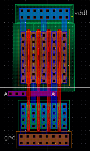
I DRCed the layout and it had no
errors.

I then performed an LVS
of the schematic view of the inverter with m=4 versus the extracted view of the
layout and saw that they corresponded with matching nets.

Part
3: Simulations, Spectre and UltraSim
Simulation
Methodology:
I used a variable for
the capacitor size to maximize efficiency and save time. I simulated the
schematic using parametric analysis of a decade and a step size of 1, driving
loads of 100fF, 1pF, 10pF, and 100pF. Using a decade analysis with a step size
of 1 simply measured increments of a decade starting from 100fF and resulted in
measurements of all four capacitor values on the same graph. I created the
variable, used the model libraries, choose the nets on the schematic and ran
the parametric analysis.
I used the same
technique for the UltraSim measurement of this
inverter, as well as the other two simulations using the 48u/24u inverter.
Ultra sim is used for simulating large circuits since spectre
is very slow when simulating large circuits. Ultrasim
simulations are usually not as accurate as the ones in spectre.
Here there is not much a difference since the simulation is not very large.
*******************
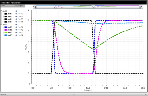
For
the 12u/6u inverter:
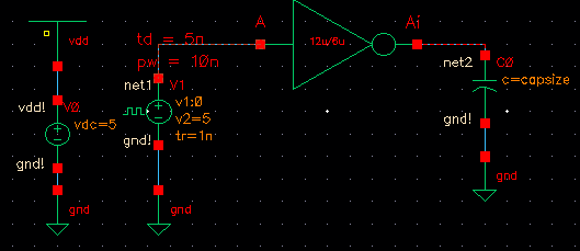
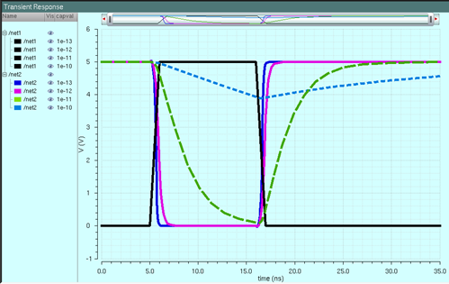
Below is the regular
simulation using spectre_state. It shows net1 as the
input which his the black line and all of the
different outputs that come with the pulsing voltage source.
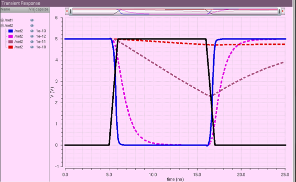
Below is the UltraSim simulation. Both are generally the same, however
the UltraSim simulation looks a little cleaner.
For
the 48u/24u inverter:
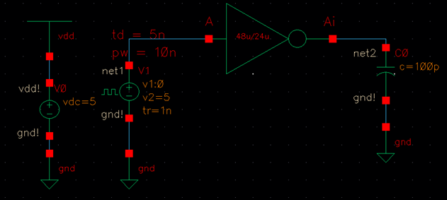
Below is the simulation using
spectre_state and the same parametric analysis
described earlier.
The results are the same as seen above. Net 1 is the input
and net 2 is the output.
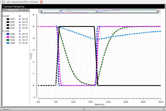
Below is the same schematic
simulated using UltraSim.
I zipped up my
Cadence files and put them in my Google drive.
