EE 421L Digital Integrated Circuit Design - Lab 4
IV
characteristics and layout of NMOS and PMOS devices in ON's C5 process
Shadden
Abdalla
September 19,
2018
About this
lab:
This lab has 6
parts:
Two NMOS
schematics –
1.
Generate a schematic for simulating ID v. VDS of an NMOS device
for VGS varying from 0 to 5V in 1Mv steps.
2.
Generate a schematic for stimulating ID v. VGS of an NMOS device
for VDS= 100Mv where VGS varies from 0 to 2 V.
Two PMOS
schematics –
1.
Generate a schematic for simulating ID v. VSD of a PMOS device for
VSG varying from 0 to 5V in 1mv steps.
2.
Generate a schematic for simulating ID v. VSG of a PMOS device for
VSD = 100mv where VSG varies from 0 to 2V in 1mv steps.
Layout –
1.
A 6u/ 0.6u NMOS device and connect 4 MOSFET terminals to probe
pads and directly adjacent to the MOSFET, DRC and LVS.
2.
A 12u/0.6u PMOS device and connect all 4 MOSFET terminals to probe
pads, DRC and LVS.
Pre-lab work:
Go through
tutorial 2:
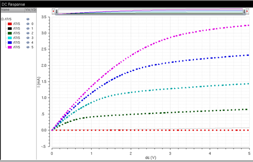
Above is the sim_PMOS_IV. Below is the simulation result of the
parametric analysis.
Above is the sim_PMOS_IV. Below is the simulation result of the
parametric analysis.
ACTUAL LAB WORK:
1.
NMOS AND SCHEMATICS
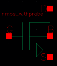
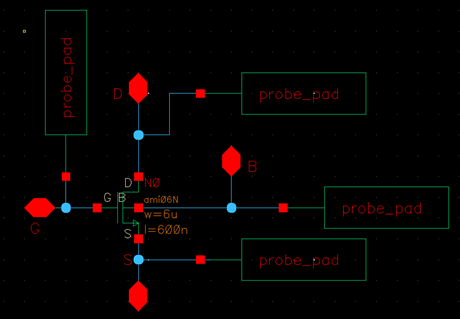
Create NMOS
symbol with probe pads. I used a 4 terminal NMOS and then connected it to the
four pins, G, D, S, B as well as a probe pad to each terminal. Then I created a
symbol for the new NMOS with the probe pads.
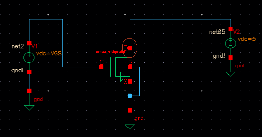
1. Schematic for
simulating ID v. VDS of an NMOS device for VGS varying from 0 to 5V in 1V steps
while VDS varies from 0 to 5V in 1mV steps. I also used an NMOS with a 6u/600n
width to length radio.
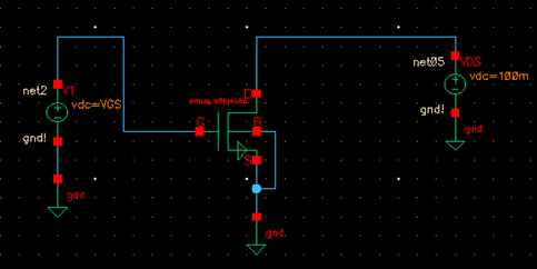
2. Schematic for
simulating ID v. VGS of an NMOS device for VDS = 100mV where VGS varies from 0
to 2V in 1mV steps.
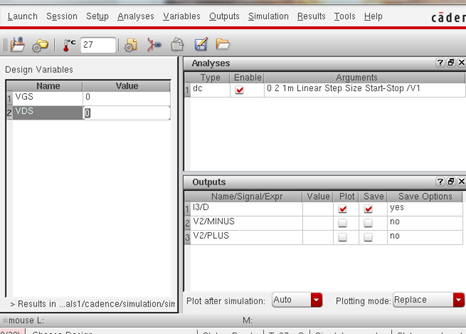
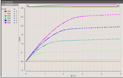
Above is the
ADE showing the step size and variables and the simulation result.
2.
PMOS AND SCHEMATICS
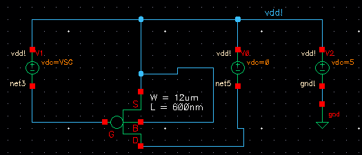
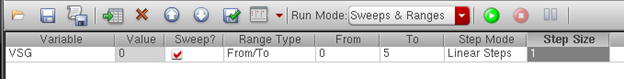
3. A schematic for
simulating ID v. VSD of a PMOS device for VSG varying from 0 to 5V in 1V steps
while VSD varies from 0 to 5v in 1mV steps.
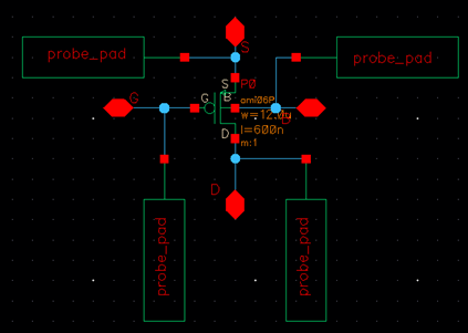
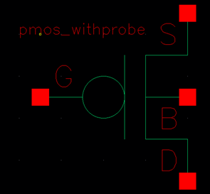
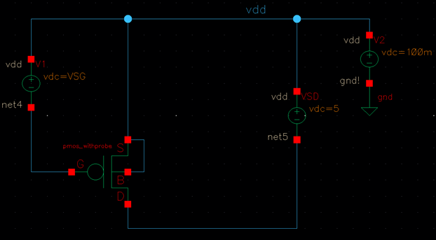
I created the
PMOS with probe pads using a 4 terminal PMOS. I connected four input-output
pins to the four terminals and then also connected the probe pads to the
terminals. Then I created a symbol for the PMOS connected to the probe pads and
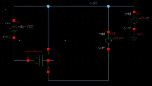
named it pmos_withprobe. On the right, I created the
schematic to test the IV curves using the new PMOS symbol. I used a variable
voltage named vdc and then used the variable VSG using a sweep from 0 to 5 to
conduct a parametric analysis on the circuit.
Above is
setting the variable voltage.
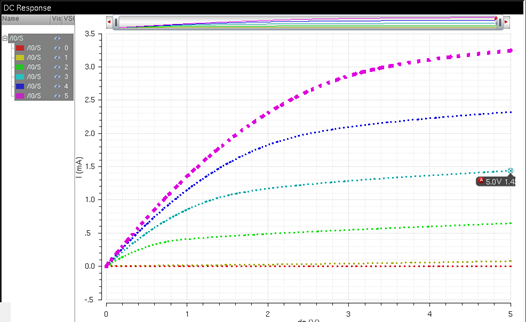
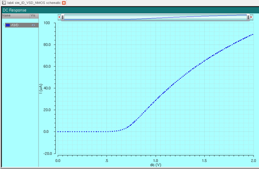
A schematic for simulating ID v. VSG of a PMOS device for VSD = 100 mV
where VSG varies from 0 to 2 V in 1 mV steps. Again, use a 12u/600n
width-to-length ratio.
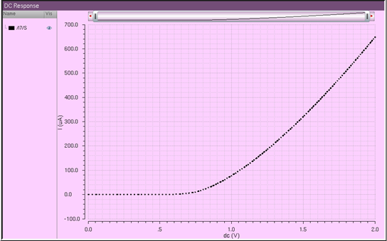
The simulation shows that the current begins to rise after staying
constant at about 0.6 volts.
NMOS LAYOUT
![]()
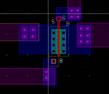
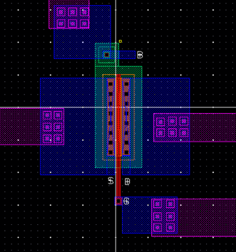
To
the left is the zoomed in layout of the middle of my NMOS. It shows the
connections from the S, G, D,
and B pins. The layout then extends to connect to the four probe
pads which is shown in the middle picture, with the light blue probe pads
connected using metal 3. I used metal one to connect the initial S, G, D, and B
pins and then connected the metal 1 pads to the metal 2 pads using vias specific to connecting metal 1 to metal 2. Then I
connected the metal 2 (pink) to metal 3 pads (light blue) in order to connect
the initial pins to the probe pads. I connected metal 2 to metal 3 using the
specific vias needed for connecting metal 2 to metal
3.
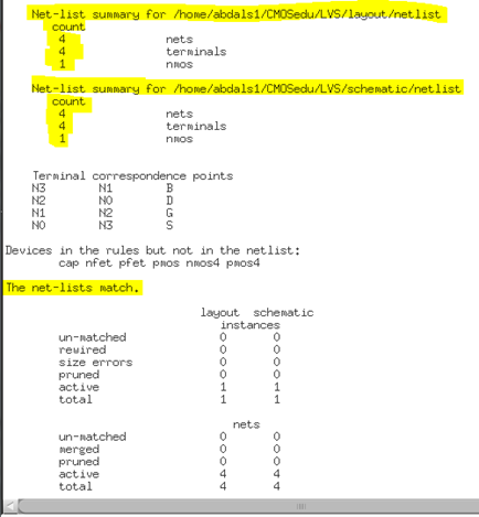
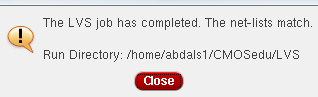
I LVS’d
and it said that the netlists match.
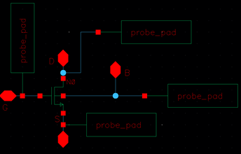
PMOS LAYOUT
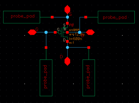
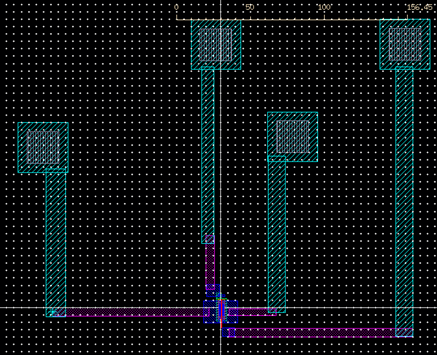

On
the left I have the regular schematic where the gates are connected to the
probe pads,
The
middle photo is the zoomed in photo of the gate. I connected the gates the same
way I connected it in the NMOS, I used metal 1 to connect to the pins, and then
used metal 2 to take us from the metal 1 pin connection to the metal 3, which
is the same metal as the probe pads. I used specific vias
to connect from metal 1 to metal 2 and other vias
specific to connecting metal 2 to metal 3 as well.
Then I performed a LVS and saw that my netlists
matched.
I zipped up my
files and put them in my google drive.
