EE 421L Digital Integrated Circuit Design -
Lab 3
Layout of a 10-bit digital-to-analog converter
(DAC)
Abdals1@unlv.nevada.edu
Lab
description:
In this lab I
will make a 10k resistor based on what I learned in tutorial one. I discuss how
to select the width and length using the information from MOSIS using the
SCMOS_SUBM-Compatible mappings. The resistors are laid out in parallel and are
stacked. I use metal one only, DRC and LVS.
Prelab: Finish tutorial 1, below is the end
of tutorial 1.
Real lab work:
Zipped up lab3.zip
– I also backed up the folder in my email.

Use the n-well
to layout a 10k resistor as discussed in Tutorial 1
Discuss in
your lab report, how to select the width and length of the resistor by
referencing the process the process information from MOSIS.
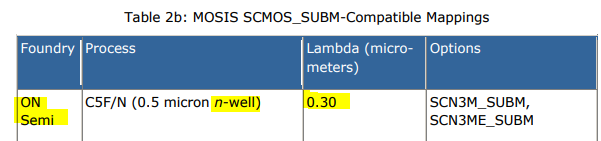
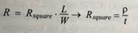
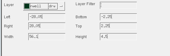
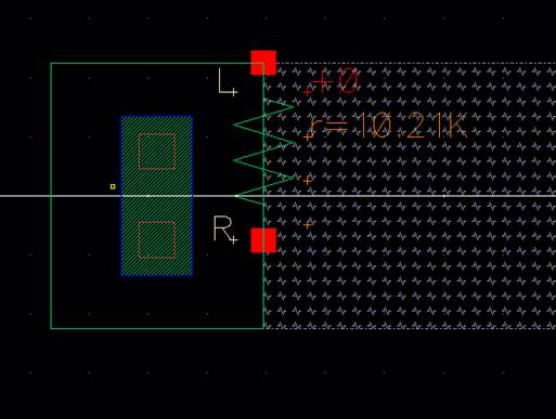
Rsquare for n-type resistors is approximately 819. I knew
that the R needed to be 10k because that is the resistance we want to layout. I
also knew that the minimum width was 4.5u so I back solved with that
information to find the ideal length which was 56um.
819*56.0um4.5um = 10.19kohms
So the length
is 56.0um and the width is 4.5um, which we decided earlier.
I created a
rectangle for the resistor and entered the dimensions we calculated. There was
an error the same way there was in the tutorial because the rectangle was not
on the grid so I added 0.05 to each of the left and right sides to remove the
error.
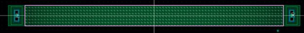
Above is the
finished resistor with the n-taps and the resistive layer on top. Below are the
pins I used, both L and R are input/output pins onto
metal 1.
I then
extracted the layout and the resistance of my rectangle was 10.21k, not exactly
the same as calculations but was instead the same way as found in the tutorial.
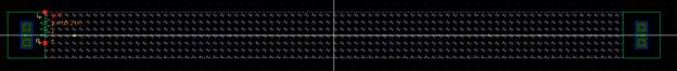
Below is the zoomed out version of the whole layout, extracted.
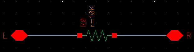
Above is the
schematic version of the resistor I just laid out showing the pins as
input/output connected to a single 10k resistor.
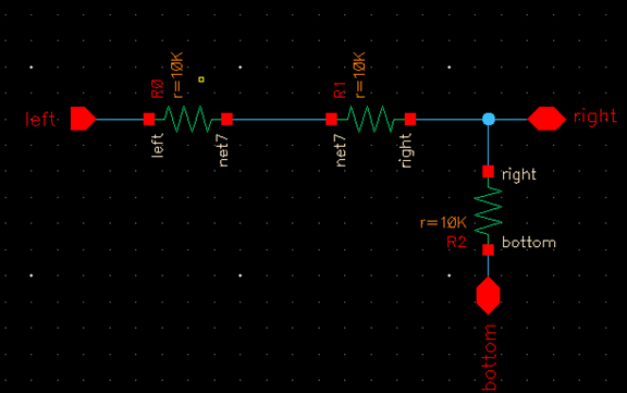
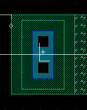
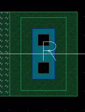
Above is the
three resistor schematic used in lab 2 to make the DAC. An input “left” goes
into two resistors connected in series, the right-most resistor outputs to
“right” and then connects to the third resistor with input/output “bottom.” The
same is relayed to the layout below. Two resistors are connected, output to
“right,” which then outputs to bottom.
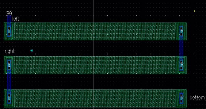
Left, right and bottom labels added for correspondence
to original schematic and will be deleted in the next step.
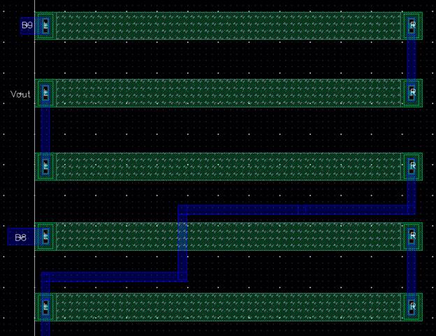
In our
original schematic, I created a symbol for the three resistors and then stacked
ten of them with another resistor on the bottom, to create the DAC. Now, I will
stack the above layout three time connecting them the same way I connected the
original schematic and then will add another resistor to ground, to the bottom.
Below is the
schematic from the DAC I made in lab 2 which shows that the bottom connects to
the right of the next block.
Below is the
entire schematic.

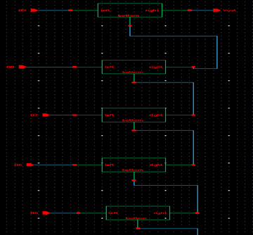
Below is the top few resistors of the schematic.
We can view
the top three resistors, and each group of three after, as one “block” of the
R-2R resistors, for which I made a symbol view in my last lab for easier
viewing. The left pin stays alone since it is an input, the right pin connects
to the third resistor, and the third resistor connects to the bottom, which
then connects to the second resistor, to the right pin. This continues on
through 10 groups of 3, until the final (31st) resistor is connected
to the bottom of the 30th resistor and is then connected to global
ground.
Below is the
last few resistors of the schematic, pin BO and the 31st resistor
connected to ground.
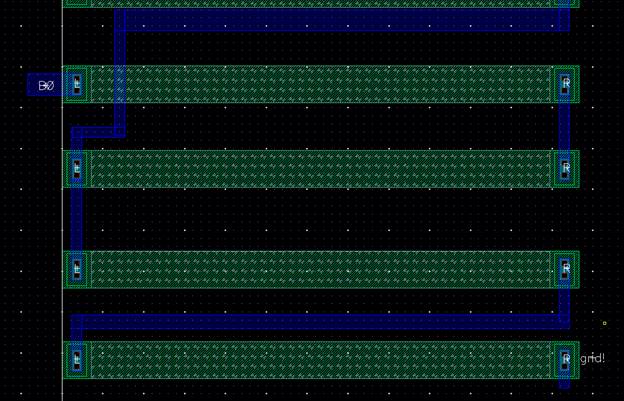
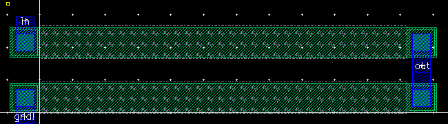
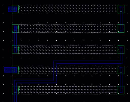
Below is the
entire layout.

Below is part
of the extracted view of part of the DAC.
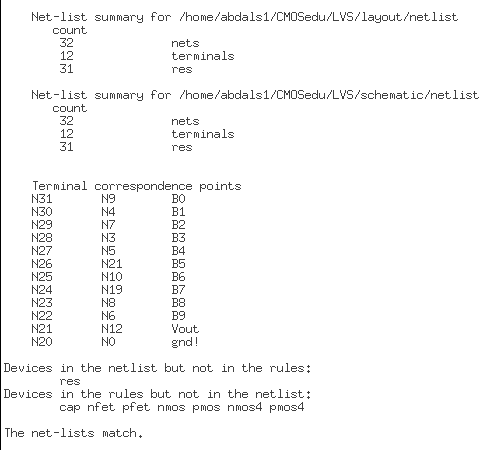
I then LVS’d the extracted view and compared it to the schematic
view of the original ten bit DAC that I made in lab 2.
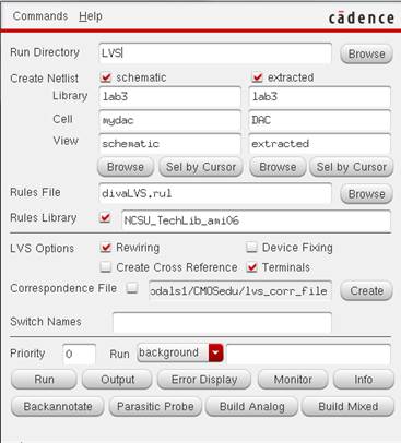
The LVS was
successful and the netlists matched.