|
Project: Design, layout, and simulation of an Even Parity Checker - EE 421L Author: Mario Verduzco Email: Verdum1@unlv.nevada.edu 11/21/17
|
|
Project description:
|
|
Project Design:
|
|
The objective of this project is to design an even parity checking circuit that has a 9-bit input, 8-bits data and 1-bit parity. This circuit should output a 1 when the even parity check is valid, and output 0 when the parity check is invalid |
|
Using a group of NOR gates it is possible to create a parity generating circuit. Which will output a 1 when there is an odd number of 1’s in a sequence. |
|
8-bit Parity Generating circuit |
|
Link to download the zip file of my Cadence simulations, layouts, and schematics: EE421L_Project |
|
8-Bit Parity Checker Symbol |
|
8-Bit Parity Checker Schematic |
|
2-input XOR schematic |
|
2-input XOR Symbol |
|
Even Parity Checker Schematic and Simulation 1 |
|
Buffer Schematic |


|
From the Parity Generating circuit we can compare that output with a Parity input using an XOR gate and Inverter that will output a valid or invalid check depending on the sequence of numbers placed on the input. |


|
Even Parity Checker Schematic and Simulation 2 |

|
8-Bit Parity Checker Truth Table |
|
The first simulation we will test the number 11011100 on the input which has an ODD number of 1’s, so we expect a valid check when Parity is 1, and that is what we see in the simulation. |
|
For the second simulation we will test the number 11111100 on the input which has an EVEN number of 1’s, so we expect a valid check when Parity is 0, and that is what we see in the simulation. |
|
P |
|
P |
|
Check |
|
Check |
|
When implementing the Parity Checker it is important to add a Buffer in order to connect it to a Bond pad and be able to drive the signal off chip. |

|
Buffer Symbol |

|
*Note “EVEN” or “ODD” refers to the number of 1’s |
|
Layout and Extracted Views |
|
The layout of the even parity checker has been done so using the method of standard cell frames. |
|
Layout of XOR gate used in the Parity Checker |

|
Layout of Buffer used in the Parity Checker |

|
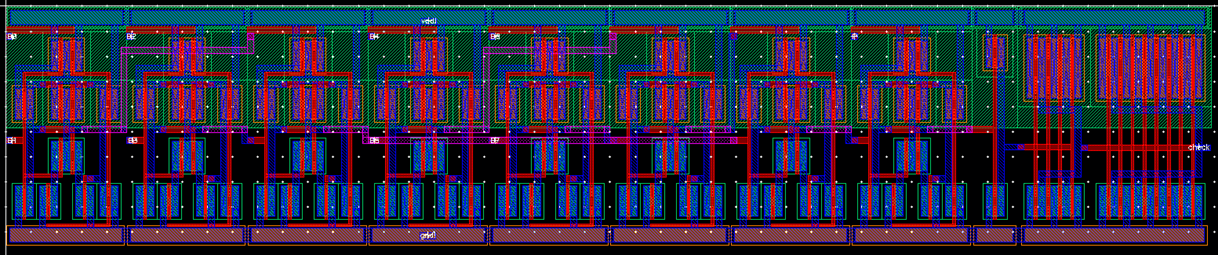
Layout of Parity Checker |
|
Extracted view of Parity Checker |

|
Parity Checker DRC and LVS |

|
Parity Checker Extracted simulation Schematic |

|
Parity Checker Extracted simulation |

|
P |
PGen |
Check |
|
0 (EVEN) |
0 (EVEN) |
1 (VALID) |
|
0 (EVEN) |
1 (ODD) |
0 (INVALID) |
|
1 (ODD) |
0 (EVEN) |
0 (INVALID) |
|
1 (ODD) |
1 (ODD) |
1 (VALID) |