EE 421L: Digital Integrated Circuit Design Lab - Lab 8
Mario
Verduzco, verdum1@unlv.nevada.edu
Gonzalo
Arteaga, arteag1@unlv.nevada.edu
Due Date: 12/6/2017
Link to directory: <<chip3_f17
>>
|
Chip Layout |
Chip Schematic |
Pin Diagram
|
Pin<1> |
Input to NAND, NOR, inverter |
|
One end of 25k resistor |
Pin<40> |
|
Pin<2> |
Input to NAND & NOR |
Junction between 10k &
25k resistors |
Pin<39> |
|
|
Pin<3> |
NAND output |
One end of 10k resistor |
Pin<38> |
|
|
Pin<4> |
Inverter output |
n/a |
Pin<37> |
|
|
Pin<5> |
NOR output |
n/a |
Pin<36> |
|
|
Pin<6> |
NAND VDD |
n/a |
Pin<35> |
|
|
Pin<7> |
Inverter VDD |
Buck converter Vout |
Pin<34> |
|
|
Pin<8> |
NOR VDD |
Buck converter out |
Pin<33> |
|
|
Pin<9> |
NMOS source/drain |
Buck converter VDD |
Pin<32> |
|
|
Pin<10> |
NMOS gate |
Parity checker input P |
Pin<31> |
|
|
Pin<11> |
NMOS source/drain |
Parity checker input D7 |
Pin<30> |
|
|
Pin<12> |
PMOS source/drain |
Parity checker input D6 |
Pin<29> |
|
|
Pin<13> |
PMOS gate |
Parity checker input D5 |
Pin<28> |
|
|
Pin<14> |
PMOS source/drain |
Parity checker input D4 |
Pin<27> |
|
|
Pin<15> |
PMOS body |
Parity checker input D3 |
Pin<26> |
|
|
Pin<16> |
n/a |
Parity checker input D2 |
Pin<25> |
|
|
Pin<17> |
n/a |
Parity checker input D1 |
Pin<24> |
|
|
Pin<18> |
Oscillator VDD |
Parity checker input D0 |
Pin<23> |
|
|
Pin<19> |
Oscillator output |
Parity checker output |
Pin<22> |
|
|
Pin<20> |
Ground (p-substrate) |
Parity Checker VDD |
Pin<21> |
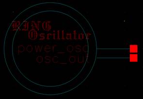
31-stage Ring Oscillator with buffer
|
Symbol |
How to test |
|
Ground pin <20> Connect 5 volt VDD to
pin<18> Measure the output at
pin<19> |
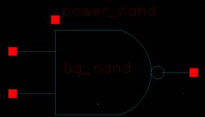
NAND Gate
|
Symbol |
How to test |
|
Ground pin <20> Connect 5 volt VDD to
pin<6> Apply inputs to pin<1>
and pin<2> Measure the output at
pin<3> |
NOR Gate
|
Symbol |
How to test |
|
|
Ground pin <20> Connect 5 volt VDD to
pin<8> Apply inputs to pin<1>
and pin<2> Measure the output at
pin<5> |
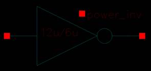
Inverter
|
Symbol |
How to test |
|
Ground pin <20> Connect 5 volt VDD to
pin<7> Apply input to pin<1> Measure the output at
pin<4> |
NMOS
|
Symbol |
How to test |
|
Ground the body at pin
<20> (Ground p- sub) Drain/Source connection at
pin<9> Drain/Source connection at
pin<11> Gate input at pin<10> |
PMOS
|
Symbol |
How to test |
|
Apply 5 volt VDD to body at
pin<12> Drain/Source connection at
pin<12> Drain/Source connection at
pin<14> Gate input at pin<13> |
Voltage Divider
|
Symbol |
How to test |
|
|
Ground pin <38> Apply input voltage to
pin<40> Measure output voltage at
pin<39> 25k resistor between
pin<40> and pin<39> 10k resistor between
pin<39> and pin<38> |
Even Parity bit checker
|
Symbol |
How to test |
|
Ground pin <20> Apply 5 volt VDD to
pin<21> Apply inputs D0:7 to
pin<23> through pin<30> Apply input parity bit at
pin<31> Measure the output at
pin<22> |
Buck Converter
|
Symbol |
How to test |
|
|
Ground pin <20> Apply 5 volt VDD to
pin<32> Place 470uH inductor across
pin<33> and pin<34> Place 4.7uF capacitor from
pin<34> to ground (pin<20>) Place load from pin<34>
to ground (pin<20>) Measure the output voltage at
pin<34> *this is designed for a
maximum load current of 100mA |
Final LVS and DRC
Return to Students
Return to Labs


