|
Lab 7: Using buses and arrays in the design of word inverters, muxes, and high speed adders - EE 421L Author: Mario Verduzco Email: Verdum1@unlv.nevada.edu 11/08/17
|
|
Pre-lab:
|
|
Lab description:
|
|
Experimental Results:
|
|
· Back-up all of your work form the lab and the course. · Read through this entire lab write-up before doing the pre-lab · Finish Tutorial 5 |
|
The objective of this lab is to design, layout, and simulate CMOS word inverter, MUX/DEMUX, and High speed adder |
|
Exercise #1 - 2 – 4Bit Word Inverter
|
|
4Bit Word Inverter Schematic |
|
Exercise #2 - 8-Bit input/output array of NAND, NOR, AND, OR, and Inverter Gates
|
|
Link to download the zip file of my Cadence simulations, layouts, and schematics: Lab7_MV |
|
Exercise #3 - Design and Simulation of 2-1 MUX/DEMUX
|
|
4Bit Word Inverter Simulation |
|
8-Bit NAND Gate Schematic |
|
8-Bit NAND Gate Symbol |
|
2-1 MUX/DEMUX Schematic |


|
8-Bit NOR Gate Schematic |
|
8-Bit NOR Gate Symbol |


|
8-Bit AND Gate Schematic |
|
8-Bit AND Gate Symbol |


|
8-Bit OR Gate Schematic |
|
8-Bit OR Gate Symbol |


|
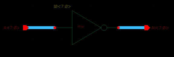
8-Bit Inverter Gate Schematic |
|
8-Bit Inverter Gate Symbol |

|
8-Bit Logic gates Schematic |

|
8-Bit Logic gates Simulation |


|
2-1 MUX/DEMUX Simulation |

|
2-1 MUX/DEMUX Truth table |
|
Exercise #4 - Design and Simulation of 8-Bit 2-1 MUX/DEMUX with a single select line
|
|
2-1 MUX/DEMUX Schematic with a single select |

|
2-1 MUX/DEMUX Symbol with a single select |


|
8-Bit 2-1 MUX/DEMUX Schematic with a single select |
|
8-Bit 2-1 MUX/DEMUX Schematic with a single select |


|
8-Bit 2-1 MUX/DEMUX Simulation |

|
Exercise #5 - Design, layout, and Simulation of 8-Bit AOI Full adder
|
|
AOI Full Adder Schematic |


|
AOI Full Adder Symbol |
|
8-Bit AOI Full Adder Schematic |

|
8-Bit AOI Full Adder Symbol |

|
8-Bit AOI Full Adder Simulation |


|
For the Word inverter the delay increased as the capacitive load increased. Additionally, The wave forms became less and less square as the capacitive load increased affecting the rise and fall time by making them longer. |
|
The 2-Bit DEMUX/MUX works by using two transmission gates with opposite inputs on each, so when the selector is high only one gate will be on. This allows the selection of two different data paths with one input. From the simulation you can see that the selector input determines which input is going to the output. The circuit can be used as both a MUX and DEMUX depending on which side is the input. |
|
This 8-Bit full adder was tested by adding the number 11100000 from input A to 00001111 from input B. The result should be 11101111 Which can be seen on the simulation. |
|
AOI Full Adder Layout and extracted view |

|
AOI Full Adder DRC and LVS |

|
8-Bit AOI Full Adder Layout and Extracted view |


|
8-Bit AOI Full Adder DRC and LVS |
|
S |
Si |
A |
B |
Z |
|
0 |
1 |
0 |
0 |
B |
|
0 |
1 |
0 |
1 |
B |
|
1 |
0 |
1 |
0 |
A |
|
1 |
0 |
1 |
1 |
A |