|
Lab 6: Design, layout, and simulation of a CMOS NAND gate, XOR gate and Full Adder - EE 421L Author: Mario Verduzco Email: Verdum1@unlv.nevada.edu 10/25/17
|
|
Pre-lab:
|
|
Lab description:
|
|
Experimental Results:
|
|
· Back-up all of your work form the lab and the course. · Read through this entire lab write-up before doing the pre-lab · Finish Tutorial 4 |
|
The objective of this lab is to design, layout, and simulate a CMOS NAND gate, XOR gate, and Full Adder using ON’s C5 process |
|
Exercise #1 - 2 – input NAND gate using 6u/.06u MOSFETs
|
|
2-input NAND Schematic |
|
Exercise #2 - 2-input XOR gate using 6u/0.6u MOSFETs
|
|
Link to download the zip file of my Cadence simulations, layouts, and schematics: Lab6_MV |
|
2-input NAND Layout |
|
Exercise #3 - Simulation of NAND gate, XOR gate, and Inverter
|
|
Exercise #4 - Full Adder
|
|
2-input NAND LVS and DRC |
|
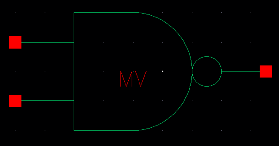
2-input NAND symbol |
|
2-input XOR schematic |
|
2-input XOR Layout |
|
2-input XOR Symbol |
|
2-input XOR LVS and DRC |
|
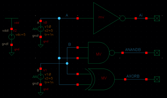
NAND gate, XOR gate, and Inverter Schematic |
|
NAND gate, XOR gate, and Inverter Simulation |
|
Truth table for NAND gate and XOR gate |
|
Full Adder Schematic |
|
Full Adder Layout |
|
Full Adder LVS and DRC |
|
Full Adder Simulation |
|
Full Adder Truth table |


|
A |
B |
A nand B |
A xor B |
|
0 |
0 |
1 |
1 |
|
0 |
1 |
1 |
0 |
|
1 |
0 |
1 |
0 |
|
1 |
1 |
0 |
1 |
|
A |
B |
Cin |
S |
Cout |
|
0 |
0 |
0 |
0 |
0 |
|
0 |
0 |
1 |
1 |
0 |
|
0 |
1 |
0 |
1 |
0 |
|
0 |
1 |
1 |
0 |
1 |
|
1 |
0 |
0 |
1 |
0 |
|
1 |
0 |
1 |
0 |
1 |
|
1 |
1 |
0 |
0 |
1 |
|
1 |
1 |
1 |
1 |
1 |