|
Lab 5: IV Design, Layout, and Simulation of CMOS Inverter- EE 421L Author: Mario Verduzco Email: Verdum1@unlv.nevada.edu 10/11/17
|
|
Pre-lab:
|
|
Lab description:
|
|
Experimental Results:
|
|
· Back-up all of your work form the lab and the course. · Read through this entire lab write-up before doing the pre-lab · Finish Tutorial 3 |
|
The objective of this lab is to design, layout, and simulate a CMOS inverter. Additionally, an Inverter that is 4 times as wide will also be designed, laid out, and simulated. |
|
Exercise #1 - 12u PMOS/6u NMOS Inverter
|
|
12u/6u Inverter Schematic |
|
Exercise #2 - ID vs VGS of an NMOS device
|
|
Link to download the zip file of my Cadence simulations, layouts, and schematics: Lab5_MV |
|
12u/6u Inverter Layout and Extracted view |
|
Exercise #3 - Simulation of 12u/6u Inverter with various loads
|
|
Exercise #4 - Simulation of 48u/24u driving various capacitive loads
|


|
12u/6u Inverter DRC |

|
12u/6u Inverter LVS |


|
48u/24u Inverter Schematic |
|
48u/24u Inverter Layout and extracted view |


|
48u/24u Inverter DRC |
|
48u/24u Inverter LVS |


|
12u/6u Inverter driving a capacitive load Schematic |
|
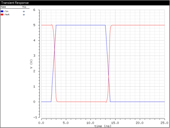
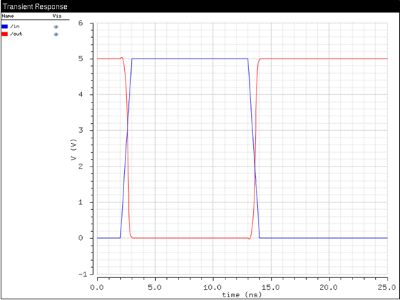
12u/6u Inverter driving a 100f load simulation |
|
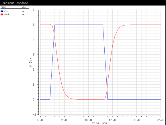
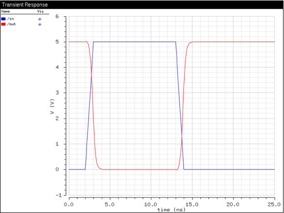
12u/6u Inverter driving a 1p load simulation |
|
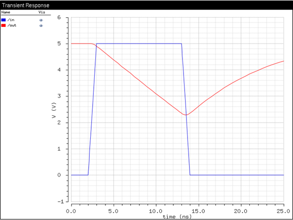
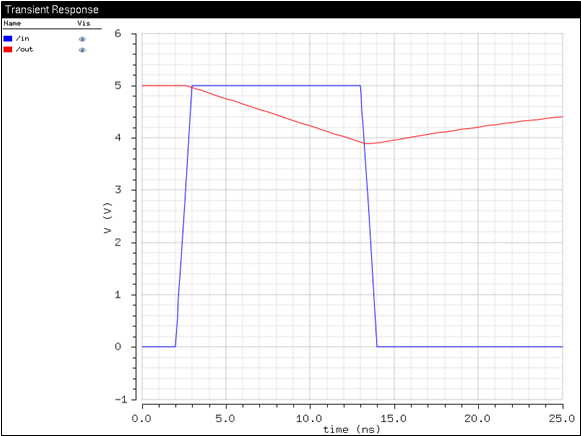
12u/6u Inverter driving a 10p load simulation |
|
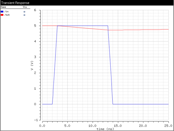
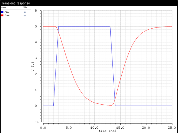
12u/6u Inverter driving a 100p load simulation |
|
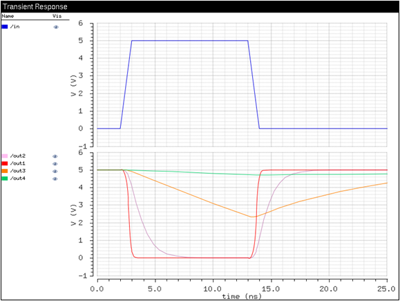
12u/6u Inverter driving capacitive loads |
|
The following Simulations were done using Cadence’s Ultrasim |
|
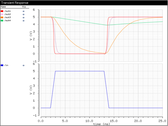
48u/24u Inverter driving a 100f load simulation |
|
48u/24u Inverter driving a 1p load simulation |
|
48u/24u Inverter driving a 10p load simulation |
|
48u/24u Inverter driving a 100p load simulation |
|
12u/6u Inverter driving capacitive loads |
|
The following Simulations were done using Cadence’s Ultrasim |
|
As the capacitive load increased the output waveform was deformed significantly. This is because the higher the capacitance is the longer the RC time constant is. Making it take longer to fill u the capacitor with charge. |
|
Similar to the previous inverter, as the capacitive load increased the output waveform was deformed significantly. However, this inverter could drive the 10pF capacitor better. This is because there is more current through the MOSFETs. |