|
Lab 4: IV Characteristics and Layout of NMOS and PMOS- EE 421L Author: Mario Verduzco Email: Verdum1@unlv.nevada.edu 09/27/17
|
|
Pre-lab:
|
|
Lab description:
|
|
Experimental Results:
|
|
· Back-up all of your work form the lab and the course. · Read through this entire lab write-up before doing the pre-lab · Finish Tutorial 2 |
|
The objective of this lab is to simulate the IV characteristics for both the NMOS and PMOS devices. Additionally, layout each device and connect the terminals to probe pads. |
|
Exercise #1 - ID vs VDS of an NMOS device
|
|
ID vs VDS Schematic: NMOS W = 6u, L = 600n
|
|
Exercise #2 - ID vs VGS of an NMOS device
|
|
DRC results shown in the command interpreter window |
|
LVS results shown in the command interpreter window |
|
Link to download the zip file of my Cadence simulations, layouts, and schematics: EE421L_Lab_4 |


|
ID vs VDS Simulation: VGS 0v to 5V
|
|
ID vs VGS Schematic: NMOS W = 6u, L = 600n
|
|
ID vs VGS Simulation: VGS= 0v to 2V, VDS= 100mV
|


|
Exercise #3 - ID vs VSD of a PMOS device
|
|
ID vs VSD Schematic: PMOS W = 12u, L = 600n
|
|
ID vs VSD Simulation: VSG= 0v to 5V
|

|
Exercise #4 - ID vs VSG of a PMOS device
|
|
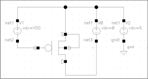
ID vs VSG Schematic: PMOS W = 12u, L = 600n
|
|
ID vs VSG Simulation: VSG= 0v to 2V, VSD= 100mV
|


|
Exercise #5 - Layout of NMOS device with probe pads
|


|
Layout of 6u/.6u NMOS device |
|
Schematic of NMOS device with probe pad pins |
|
Layout of NMOS with probe pads |


|
Exercise #6 - Layout of PMOS device with probe pads
|


|
Layout of 12u/.6u PMOS device |
|
Schematic of PMOS device with probe pad pins |
|
Layout of PMOS with probe pads |
|
DRC results shown in the command interpreter window |
|
LVS results shown in the command interpreter window |