Lab 04 - EE 421L 

Authored by Ethan Tash,

tash@unlv.nevada.edu 

09/27/2017 


Prelab:
fig%2000.PNG
fig%2001.PNG
Fig 01: My backed up work as part of the prelab instructions
 

Postlab:
fig%2003.PNG
Schematic 01:
fig%2004.PNG
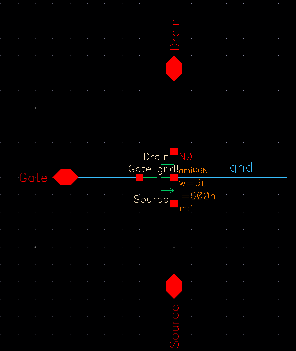
Fig 04: 6um/600nm NMOS
fig%2005.PNG
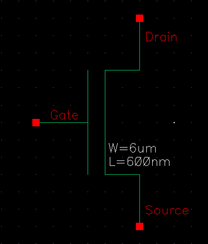
Fig 05: 6um/600nm NMOS symbol created from schematic
 
fig%2006.1.PNG
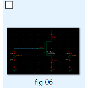
Fig 06.1: Schematic for simulating ID vs.  VDS of a NMOS device
fig%2007.1.PNG
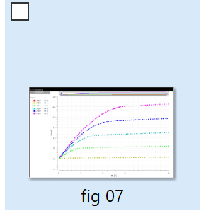
Fig 07.1: simulated results for VDS from 0 to 5V in 1mV steps
 
fig%2006.PNG
Fig 06: Schematic for simulating ID vs.  VDS of a NMOS device
 
fig%2007.PNG
Fig 07: simulated results for NMOS device of VDS from 0 to 5V in 1mV steps
 
Schematic 02:
fig%2008.PNG
Fig 08: Schematic for simulating ID vs.  VGS of a NMOS device where VDS is set to equal 100mV and VGS steps from 0 to 2V
 
fig%2009.PNG
Fig 09: simulation of ID vs.  VGS of a NMOS device where VDS is set to equal 100mV and VGS steps from 0 to 2V
Schematic 03:
fig%2010.PNG
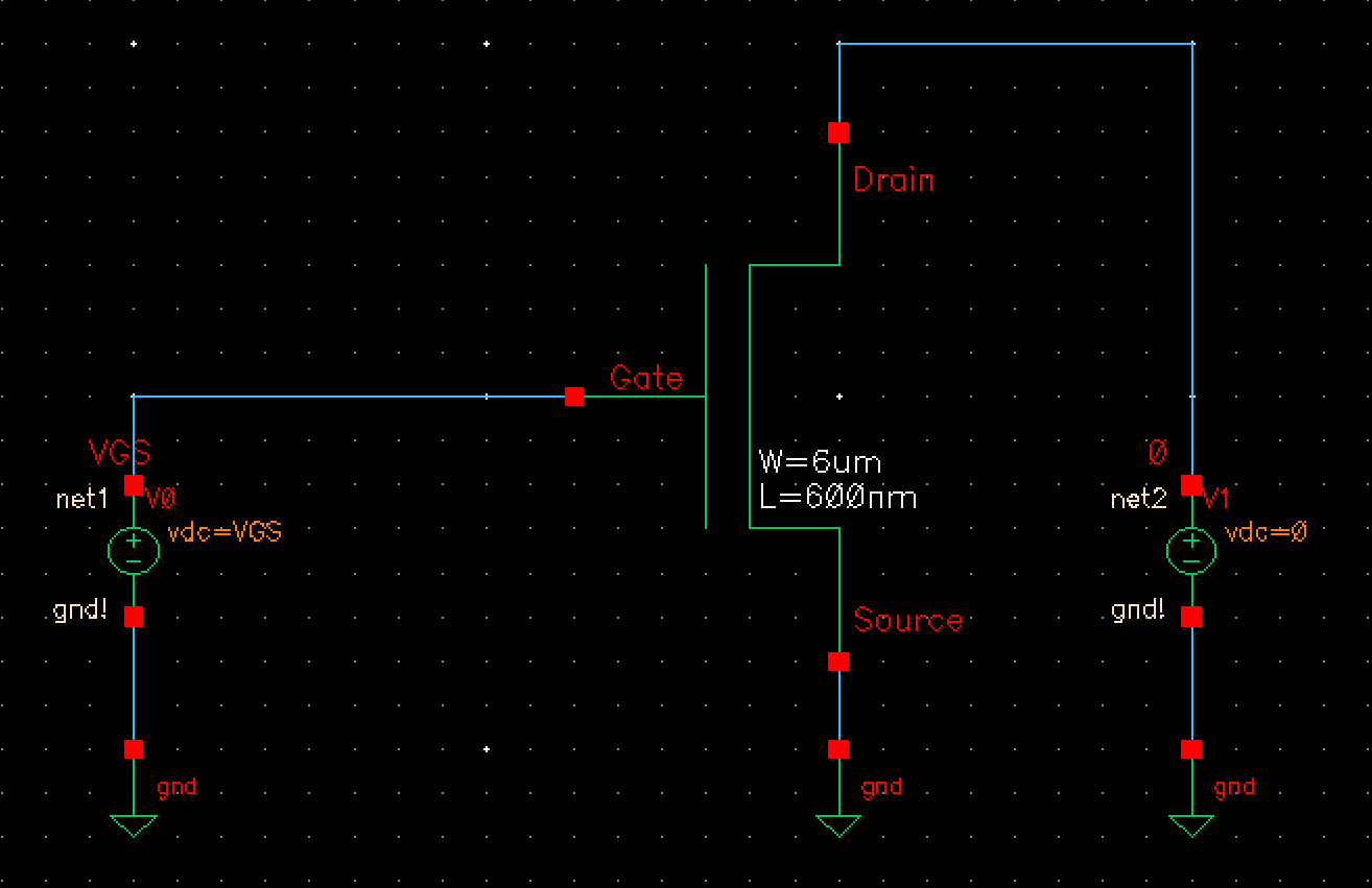
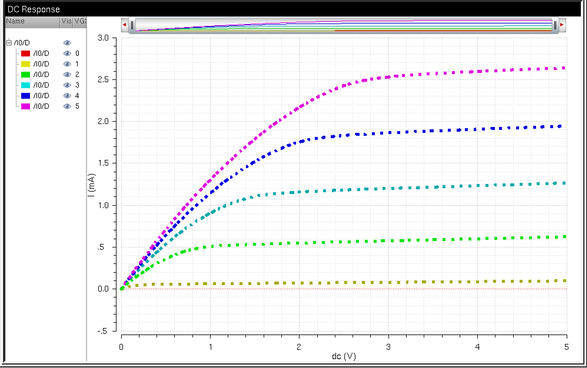
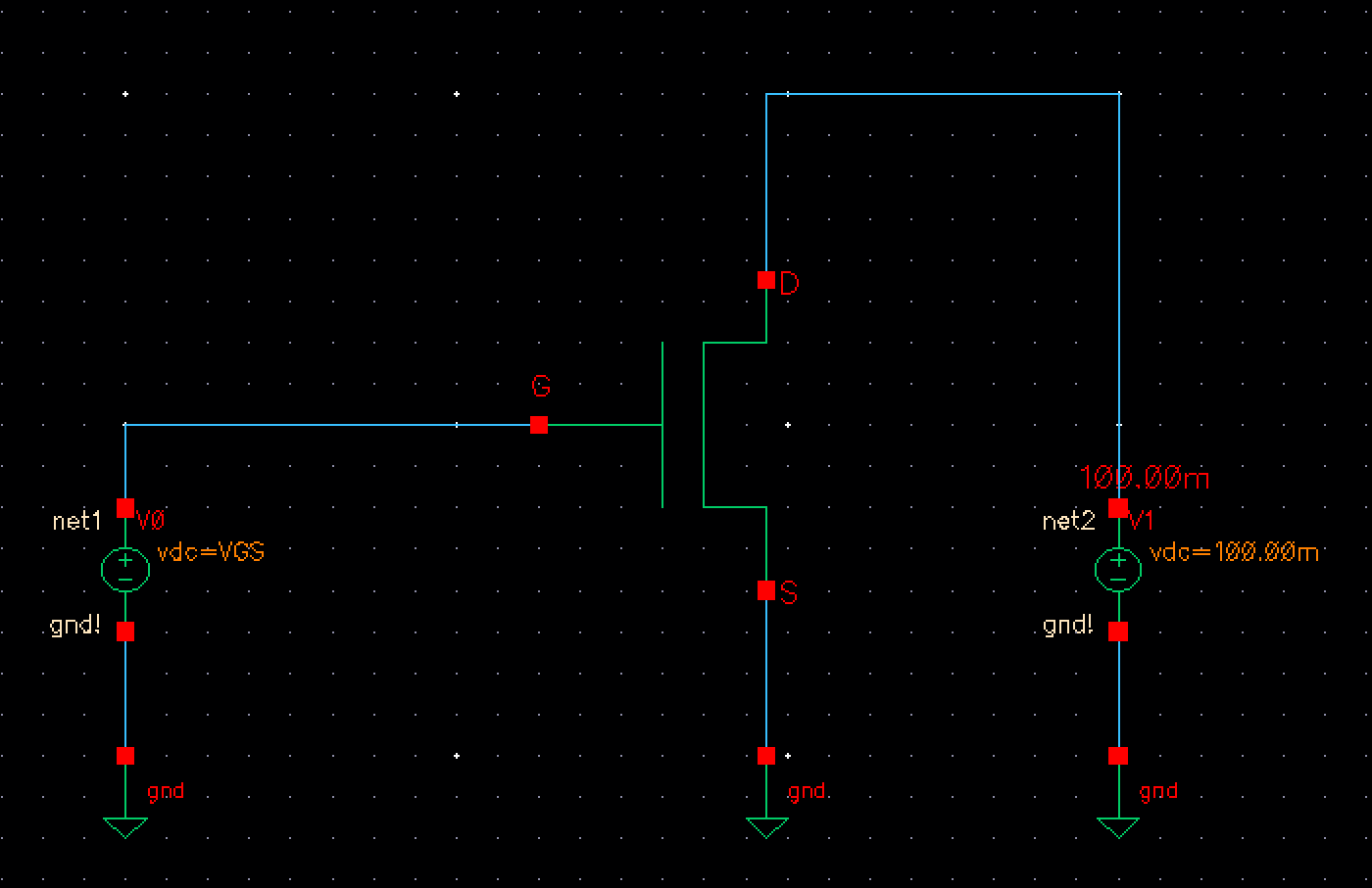
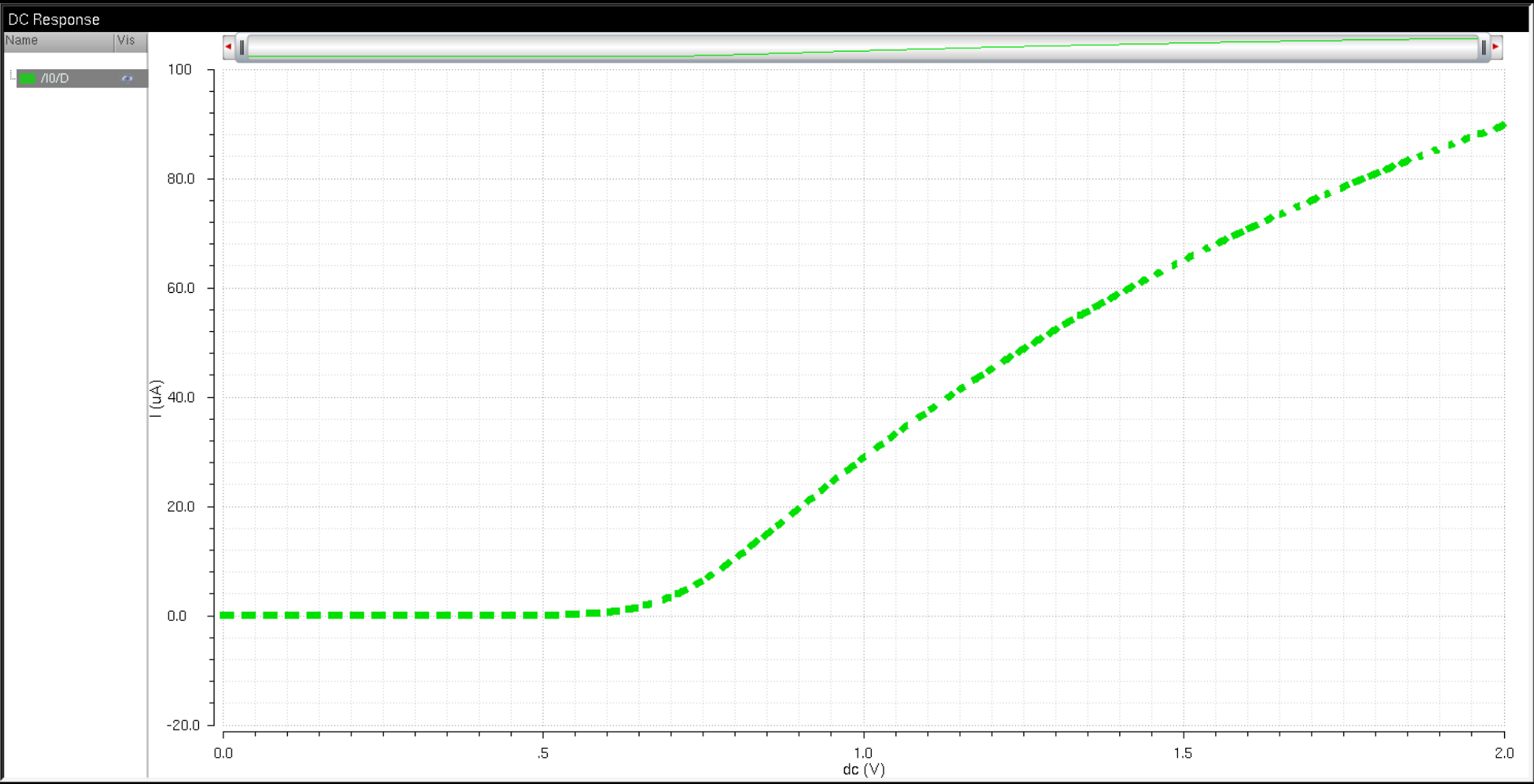
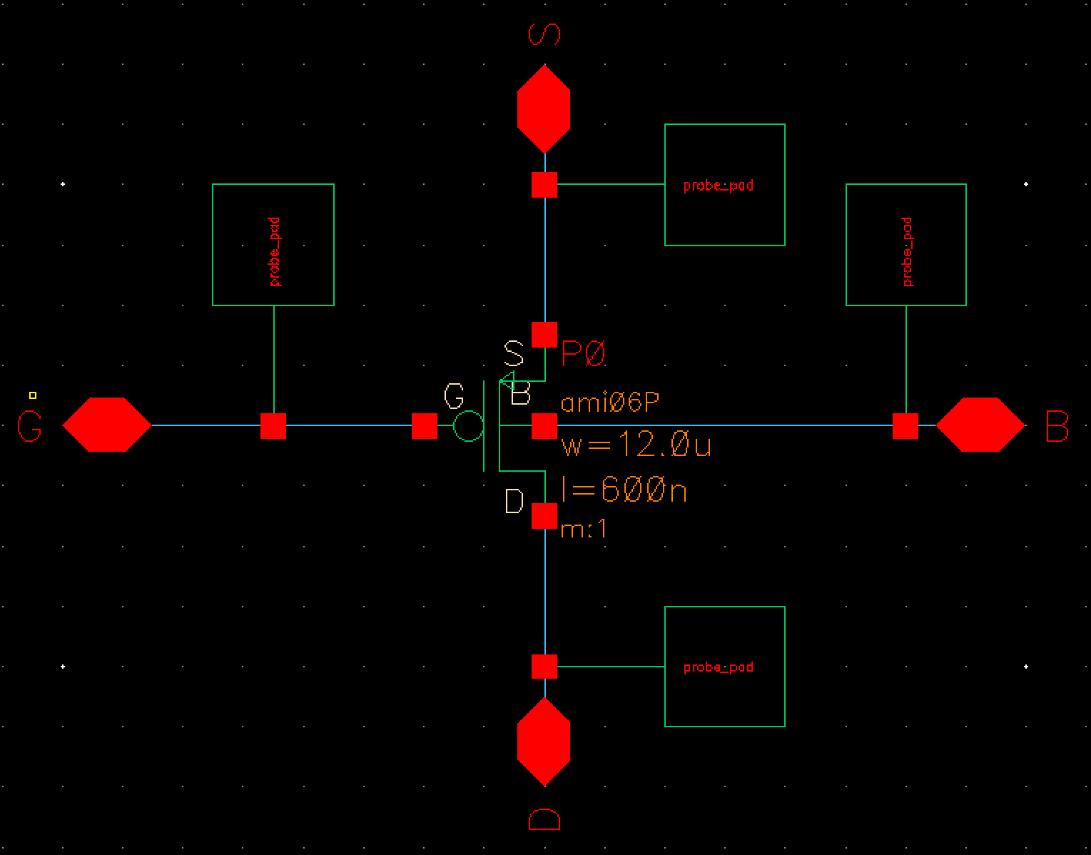
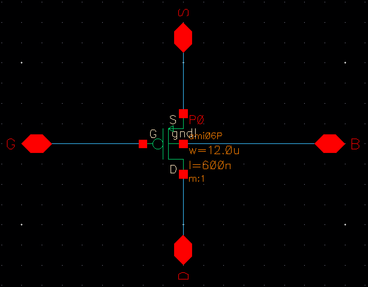
Fig 10: 12um/600nm PMOS
fig%2011.PNG
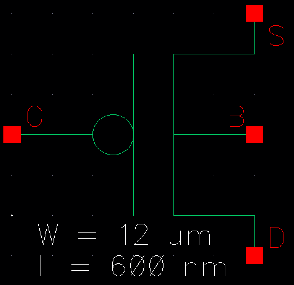
Fig 11: 12um/600nm PMOS symbol created from schematic
 
fig%2012.1.PNG
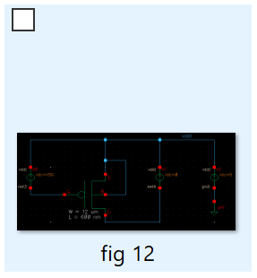
Fig 12.1: Schematic for simulating ID vs.  VSD of a PMOS device
fig%2013.1.PNG

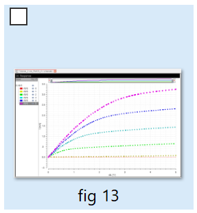
Fig 13.1: simulated results for VSD from 0 to 5V in 1mV steps
 
fig%2012.PNG
Fig 12: Schematic for simulating ID vs.  VSD of a PMOS device
 
fig%2013.PNG 
Fig 13: simulated results for VSD from 0 to 5V in 1mV steps
 
Schematic 04:
 fig%2014.PNG
Fig 14: Schematic for simulating ID vs.  VSG of a PMOS device where VSD is set to equal 100mV and VSG steps from 0 to 2V
 
fig%2015.PNG
Fig 15: Simulation ID vs.  VSG of a PMOS device where VSD is set to equal 100mV and VSG steps from 0 to 2V
 
fig%2016.PNG
fig%2016.2.PNGfig%2016.1.PNG
Fig 16.1- 16.2: MOSIS design rules found from link provided on lab 4

fig%2017.PNG
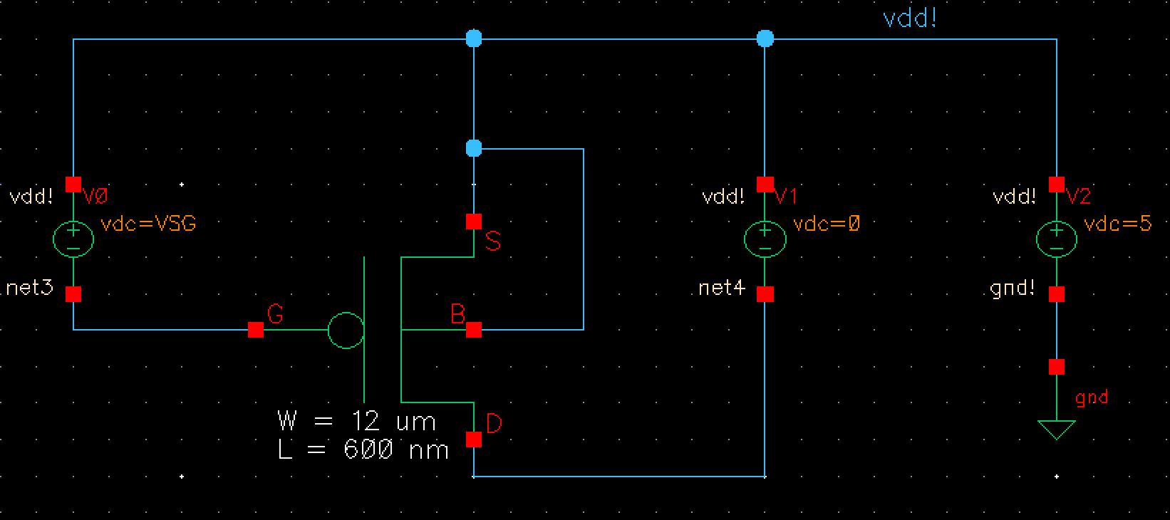
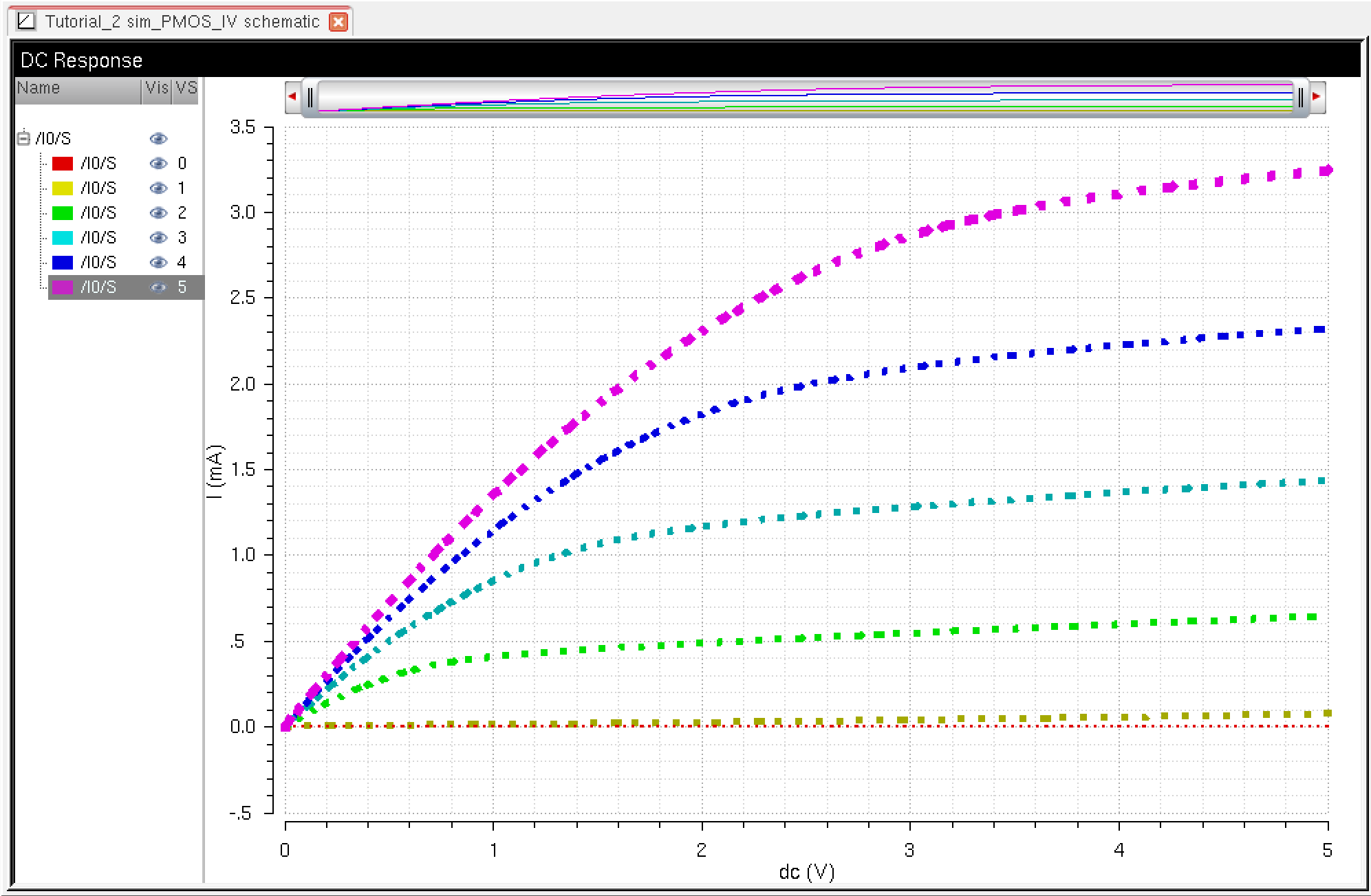
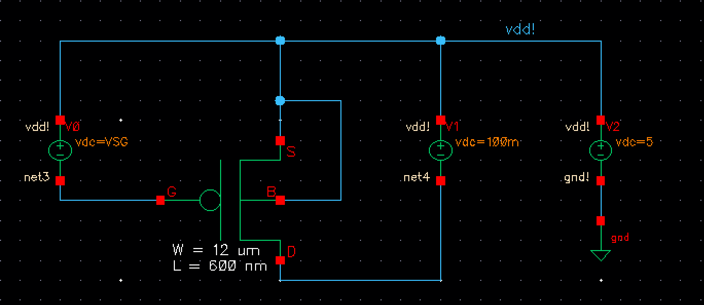
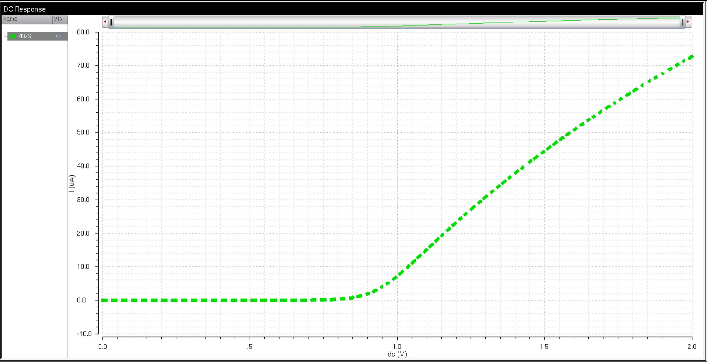
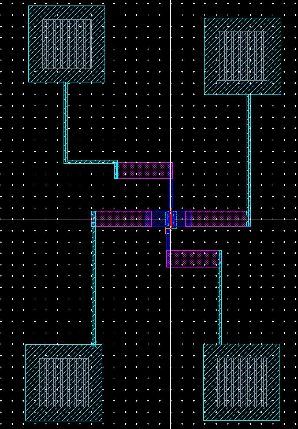
Fig 17: 6u/600n NMOS with probe pads attached layout
fig%2018.PNG
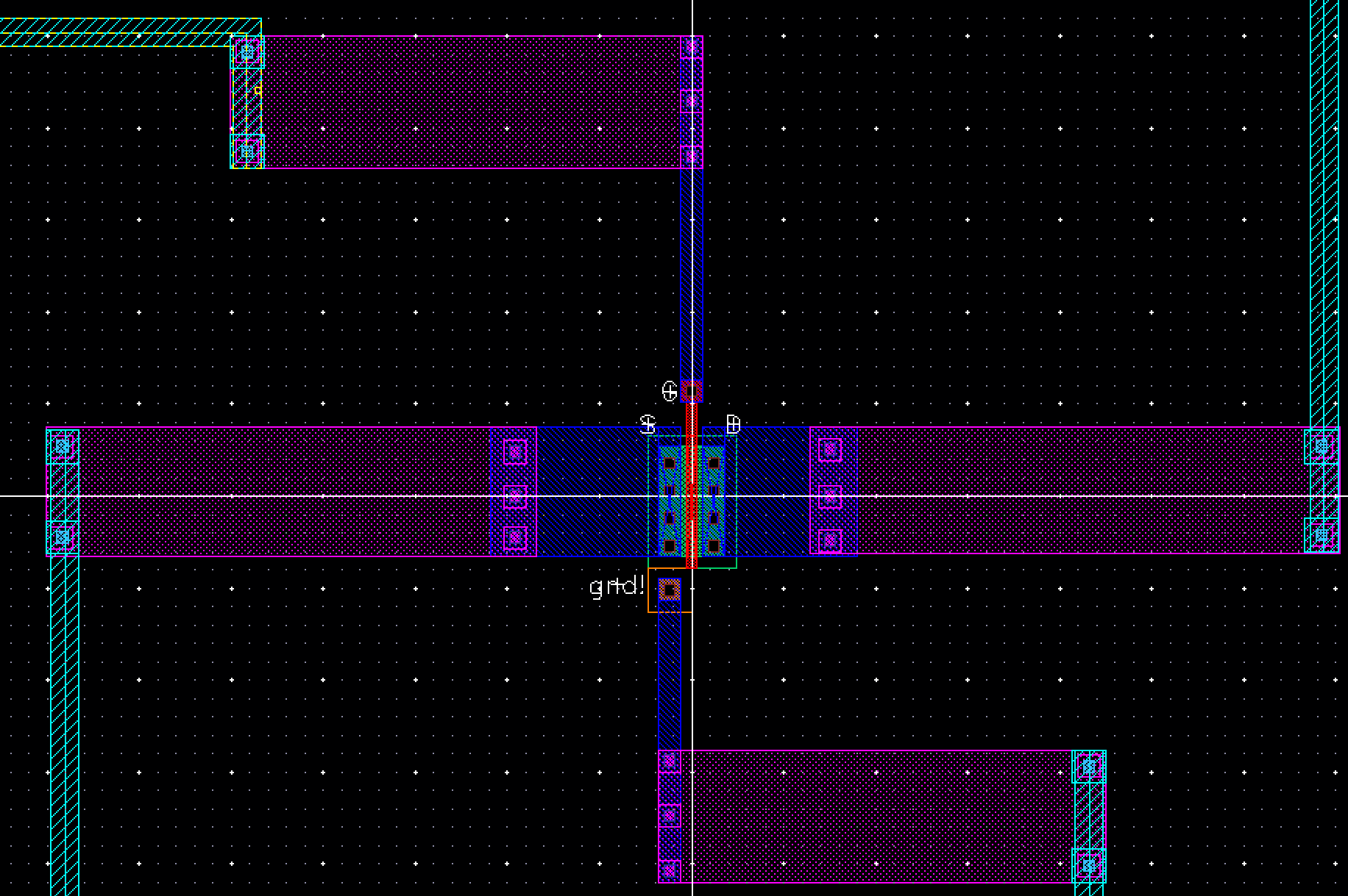
Fig 18: 6u/600n NMOS with probe pads attached extracted view

fig%2019.PNG
Fig 19: 6u/600n NMOS with probe pads attached layout DRC verification
fig%2020.PNG
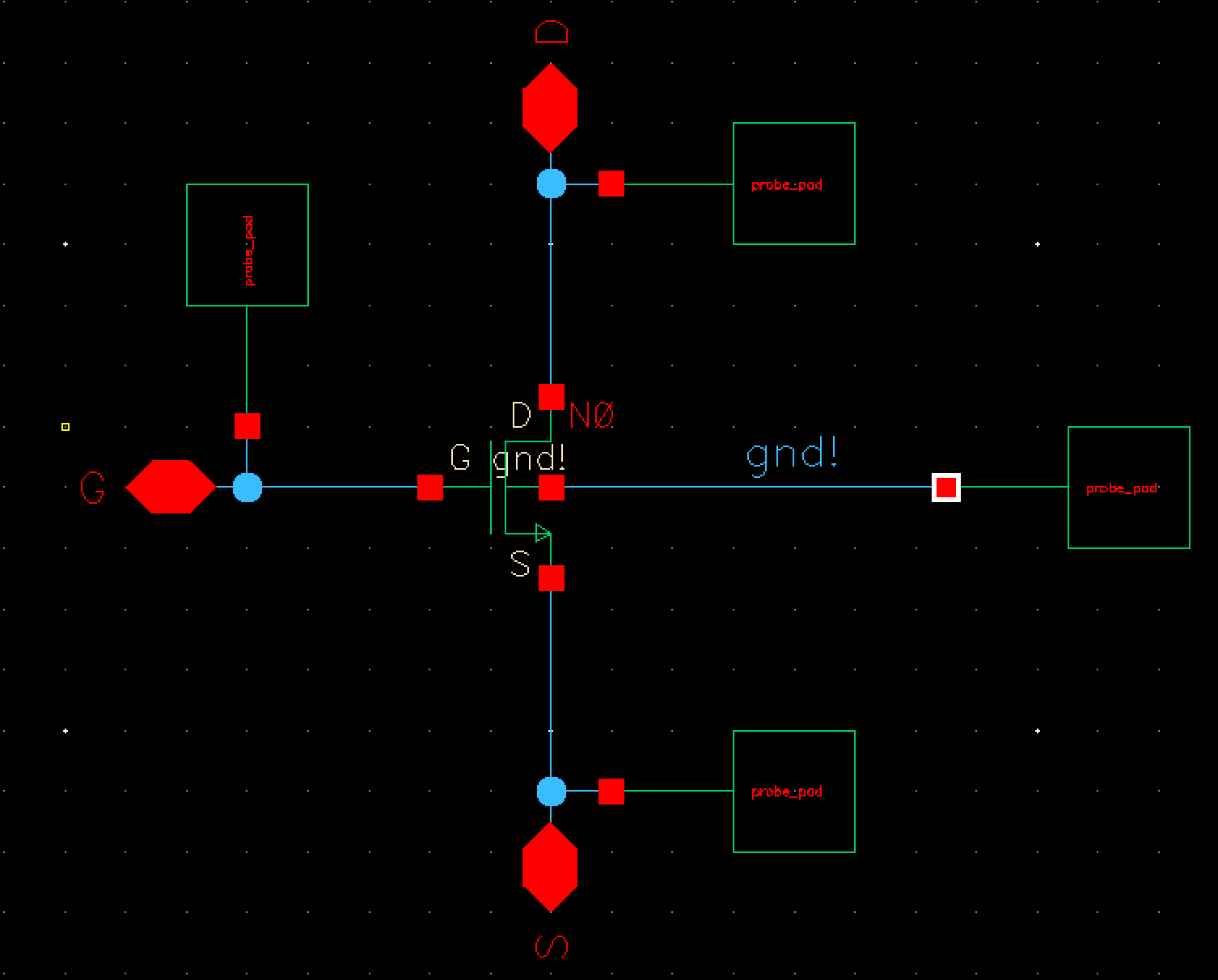
Fig 20: 6u/600n NMOS with probe pads attached schematic
 
fig%2021.PNGfig%2022.PNGfig%2023.PNG
Fig 21-23: 6u/600n NMOS with probe pads attached extracted with verification of LVS and netlists match
 
fig%2024.PNG
 
fig%2025.PNG
fig%2026.PNG
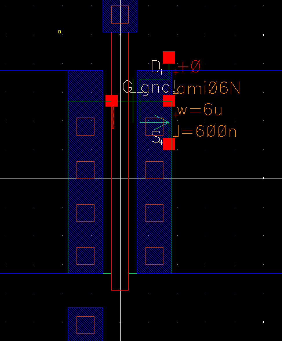
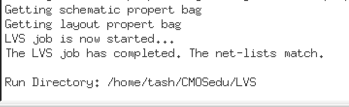
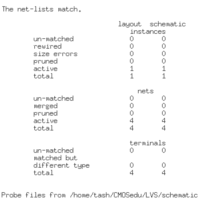
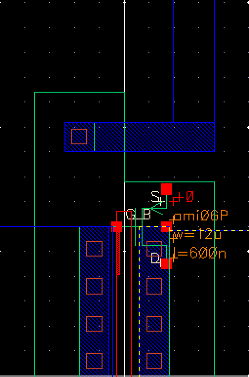
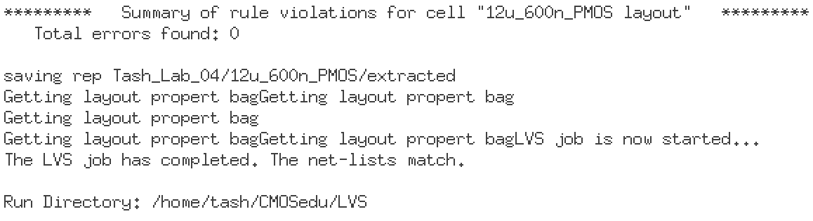
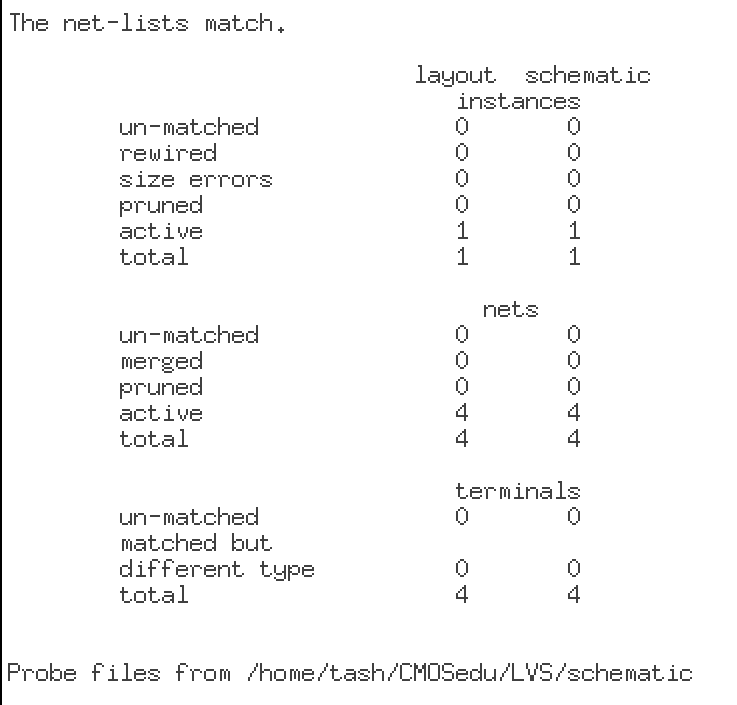
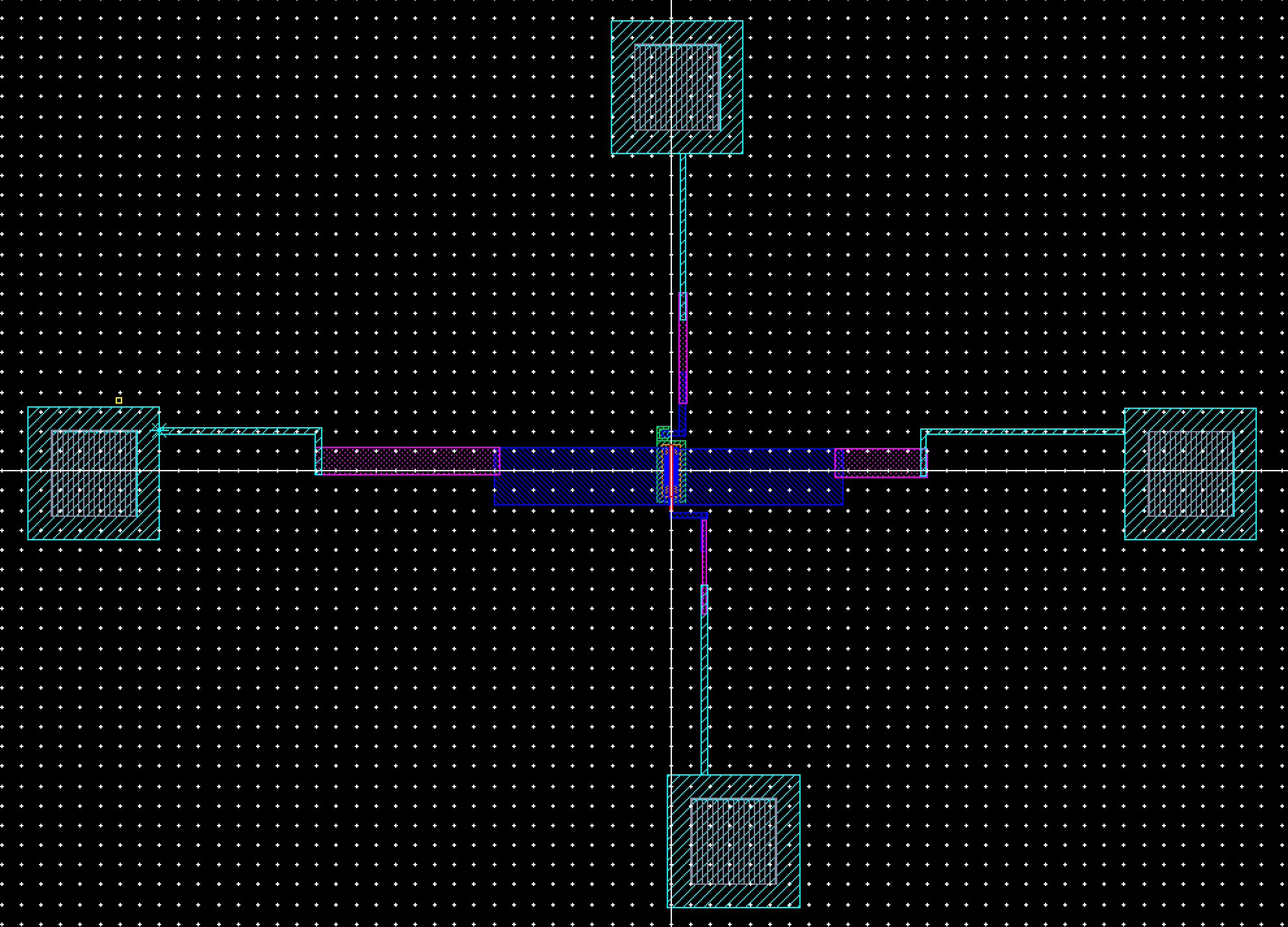
Fig 25-26: 12u/600n PMOS with probe pads attached layout and DRC verification
 
fig%2027.PNG
Fig 27: 12u/600n PMOS with probe pads attached schematic
 
fig%2028.PNGfig%2029.PNGfig%2030.PNG
Fig 28-30: 12u/600n PMOS with probe pads attached extracted view along with LVS verification and Net list match

Return to EE 421L labs