Lab 03 - EE 421L

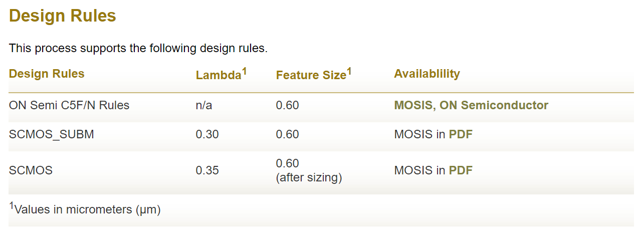
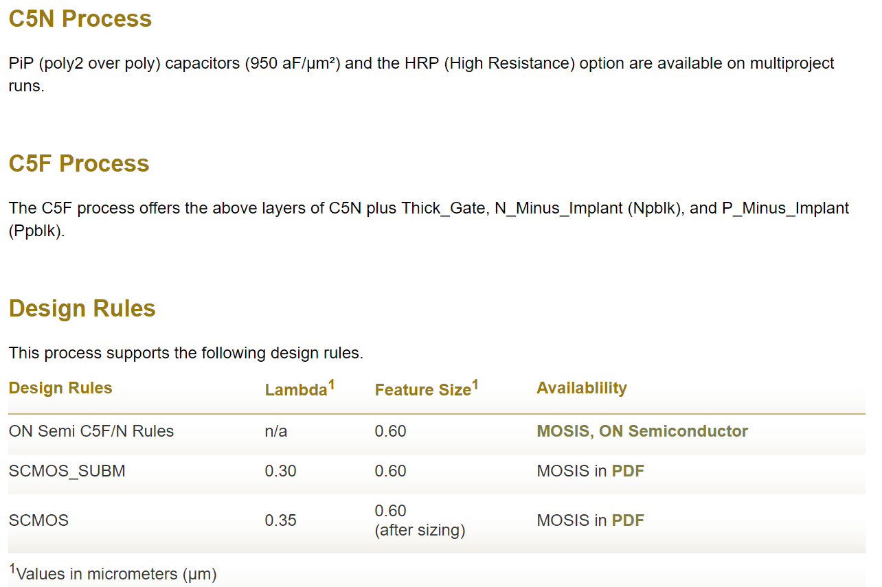
Fig 1: this is a table containing the actual design rules that we will be utilizing in both the lecture and the lab
Fig 2: additional design rules for 0.60 micrometers is provided along with links to more comprehensive documentation
As part of previous homework assignments we did calculations for a set lambda in relation to our individual designs. below are those calculations verifying
our design is within standards as the boarder is at 56.1 from edge to edge running the length of the nwell.
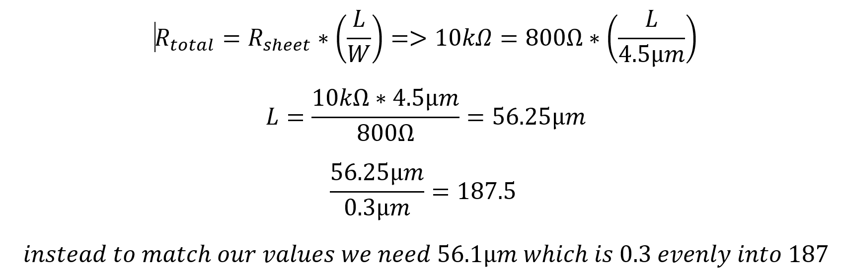
Fig 3: are the calculations verifying the design is in compliance with MOSIS design standards
The N-well resistor and the 10-bit DAC realized with 10k resistors:
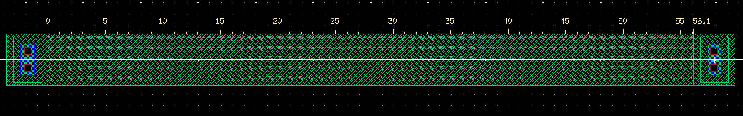
Fig 4: the n-well resistor designed within MOSIS standards using the bind key 'k' you can set a ruler or just modify within properties
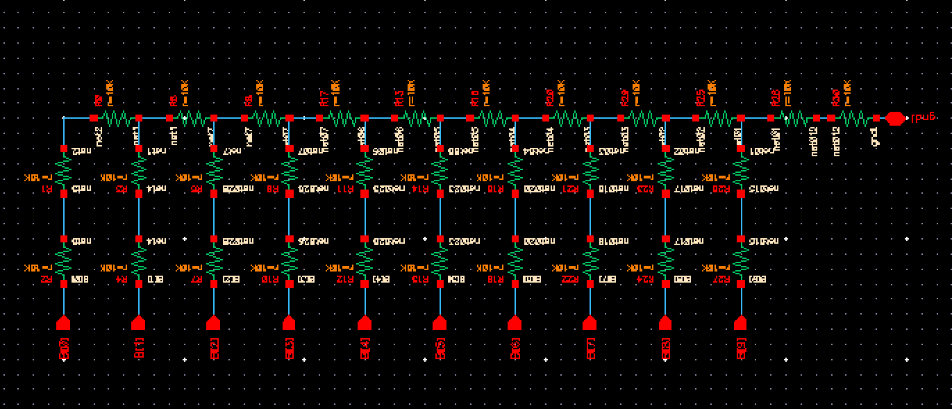
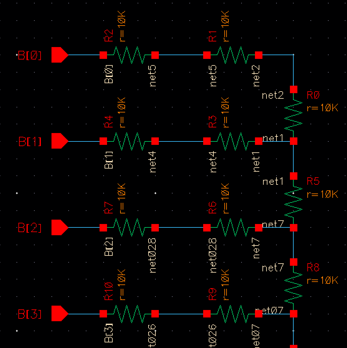
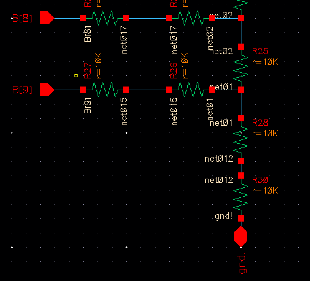
Fig 5-7: is the schematic layout for my 10-bit DAC using 10K resistors representing 2R and R from the previous lab
N-well layer for the construction of the 10-bit DAC realized with 10k n-well resistor:
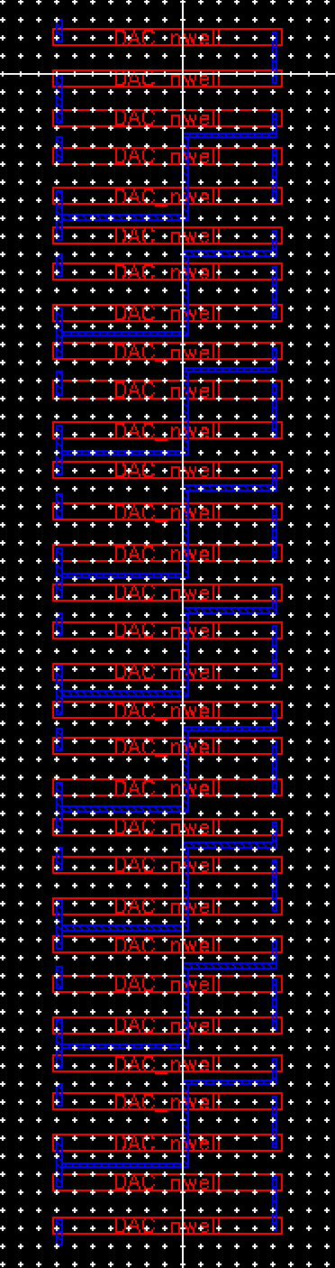
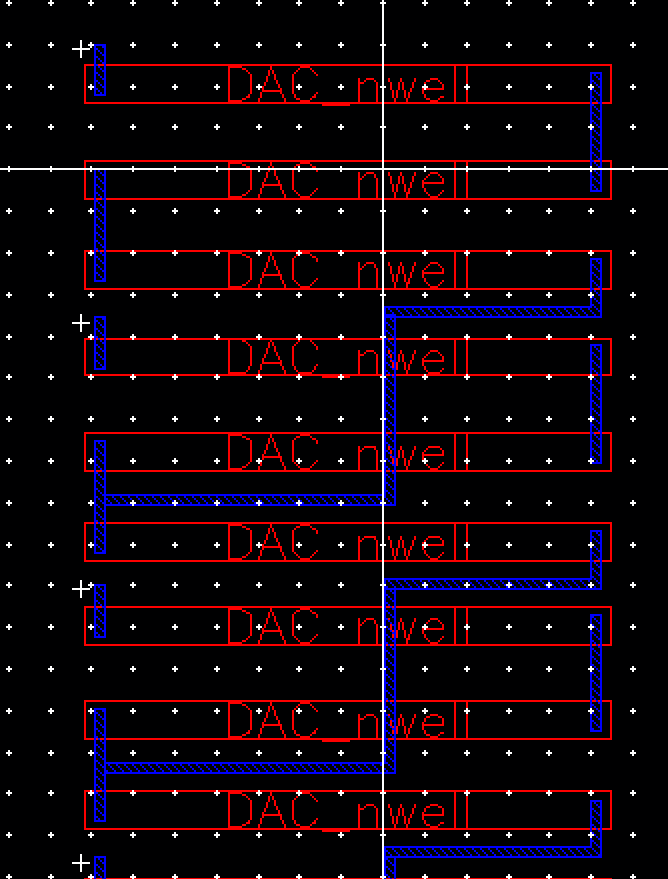
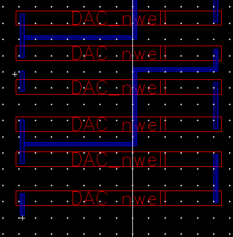
Fig 8-10: is the view of my nwell layer with the viewing set to 0 which shows only component outline
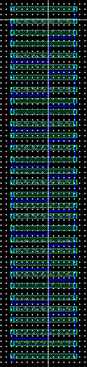
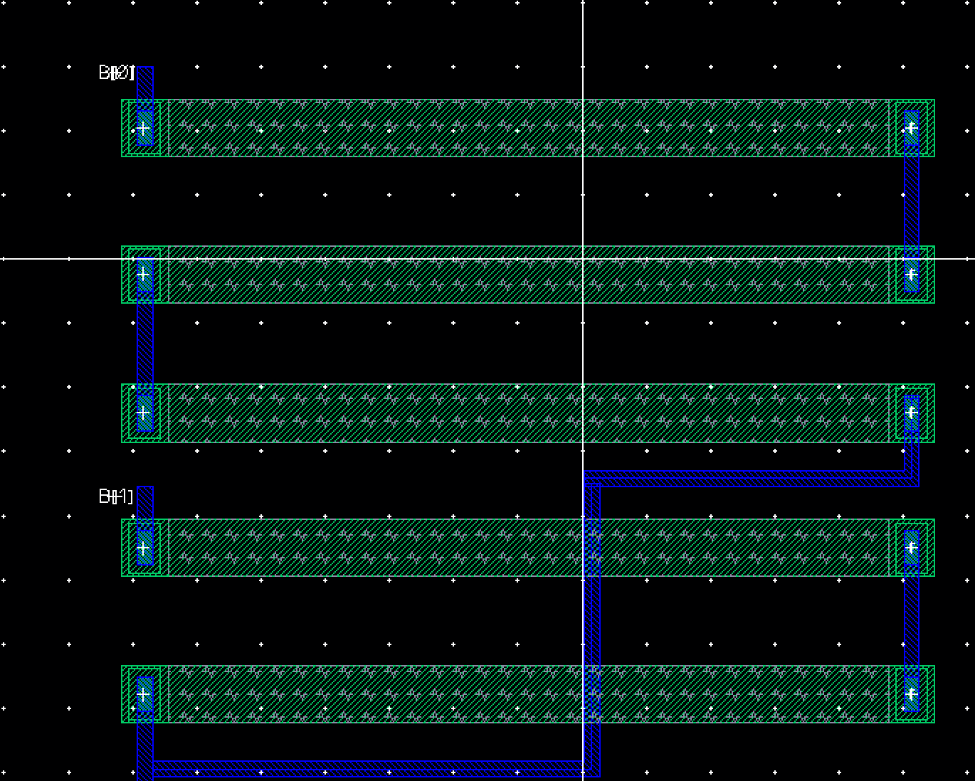
Fig 11-12: is the view of my nwell layer with the viewing set to 10
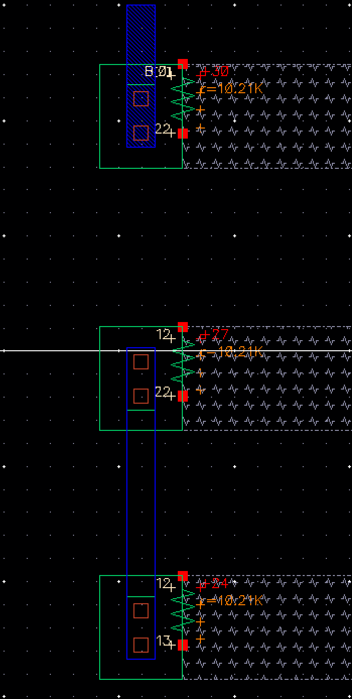
Fig 13: this is the extracted view of my nwell layer confirming equal resistance for each nwell resistor
Final Result: The LVS showed successful netlist matching
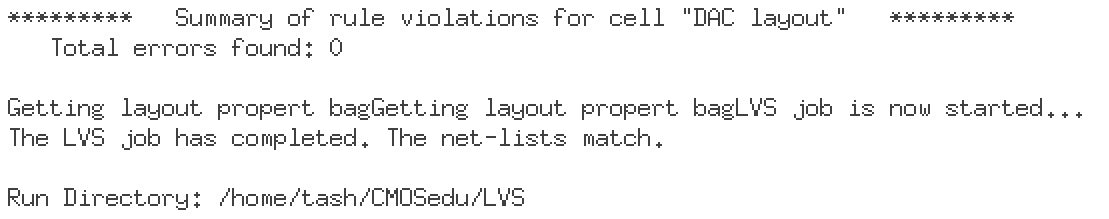
Fig 14: the confirmation of successful DRC verification and LVS
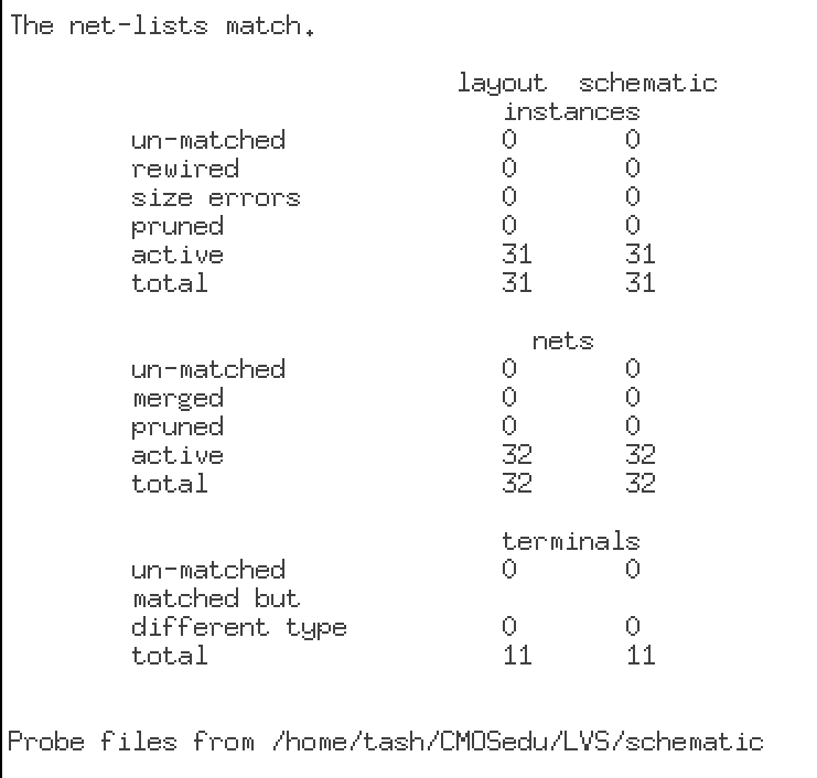
Fig 15: is from the LVS output text file showing that my netlist did indeed match
Click to Download lab 3 zip file