Lab
02 - EE 421L
Authored by Ethan Tash,
tash@unlv.nevada.edu
09/06/2017
Prelab:
For the purpose of the pre lab I initially backed up all work related to the lab and downloaded the zip file containing the lab 2 Ideal 10-bit ADC to DAC
circuit
to my CMOSedu library. I unzipped the file and ran the initial
transient response simulation. I experimented with the circuit by
initially removing the wires
connecting pin B[9:0]
Fig 0: Image of backed up zip files located in my google drive
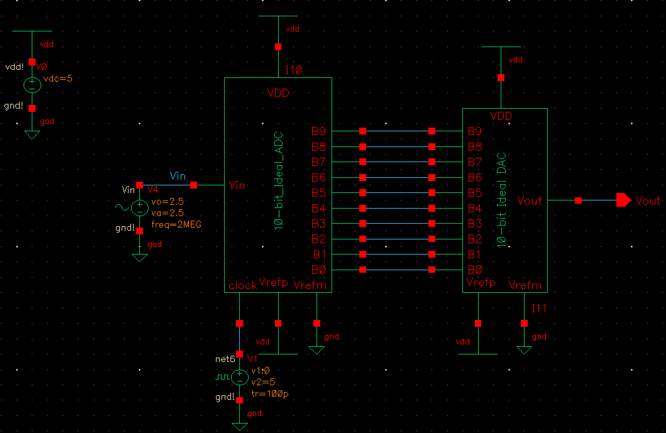
Fig 01: Schemactic of the Ideal 10-bit ADC to DAC
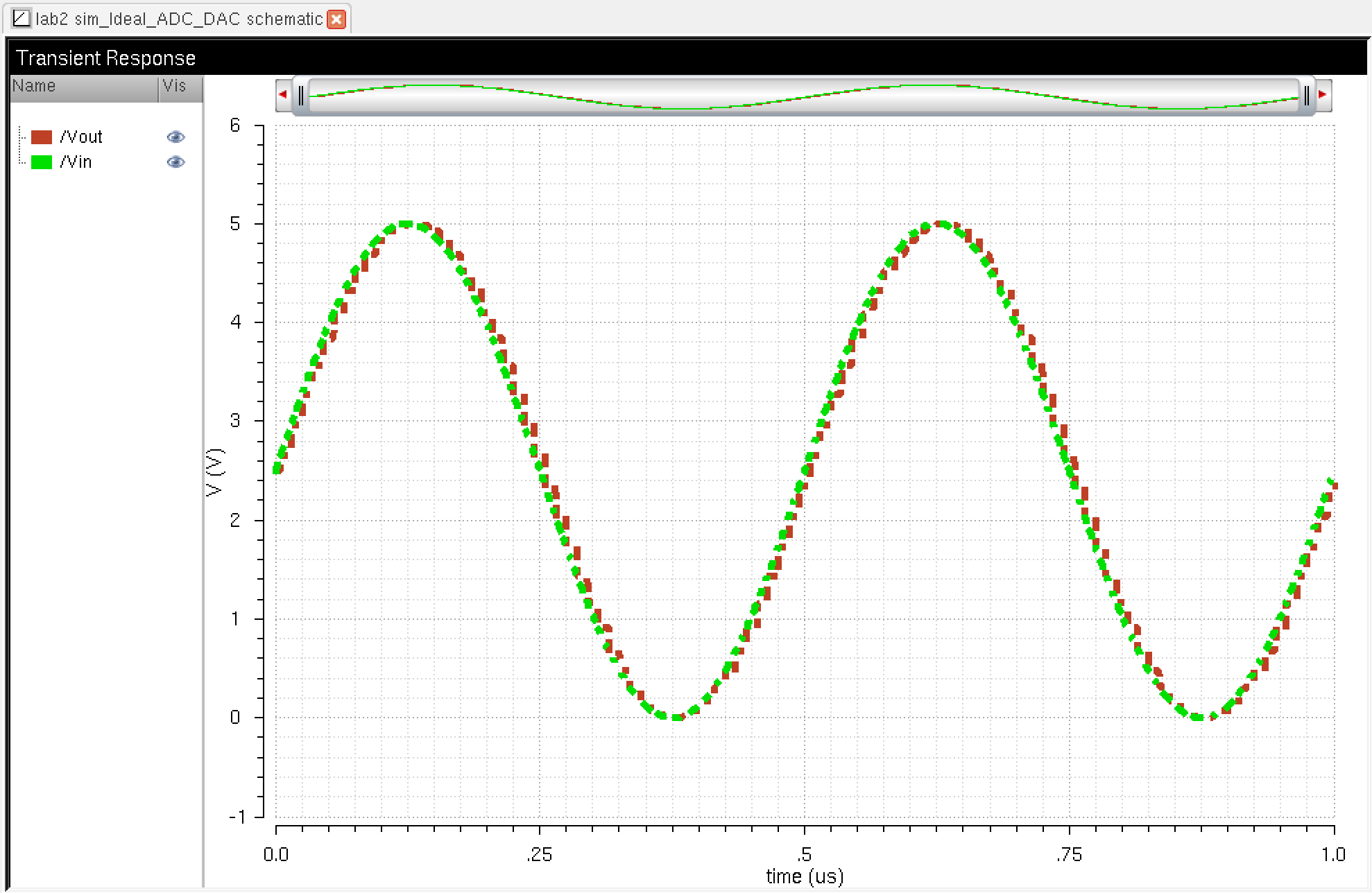
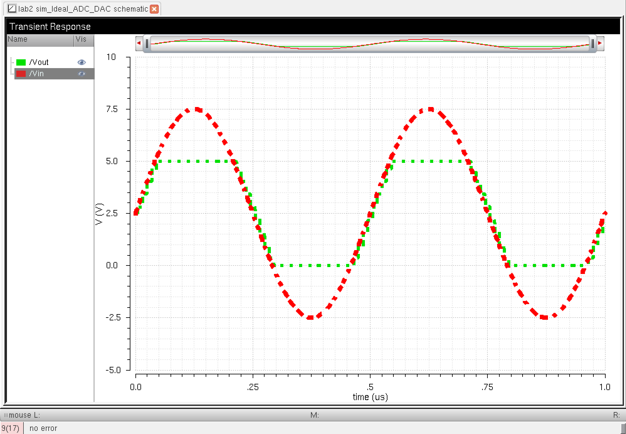
Fig 02: Simulated output for the Transient Response of the 10-bit Ideal ADC to DAC circuit
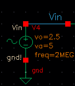
Fig
05: adjusted input voltage
Fig 04: Observed clamping of circuit if Input voltage
equals or exceeds 5V
Post Lab:
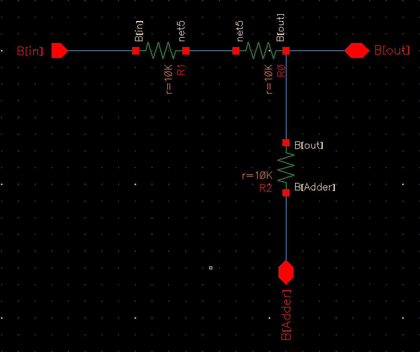
Fig
06: Voltage Divider with 2R being represented by two 10k resistors in
series which will be the N-well resistors implementing the 10 bit DAC
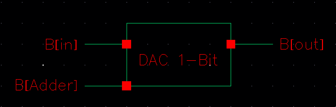
Fig 07: My custom symbol for the Voltage Divider
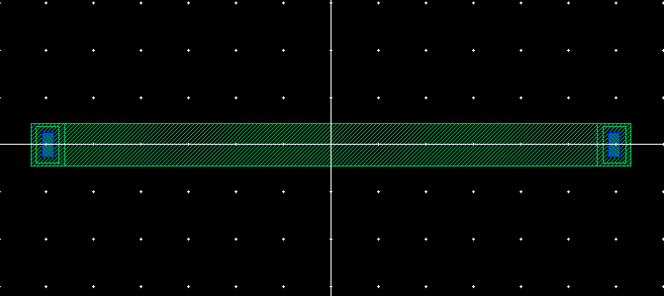
Fig 08: N-well layer resistor symbol
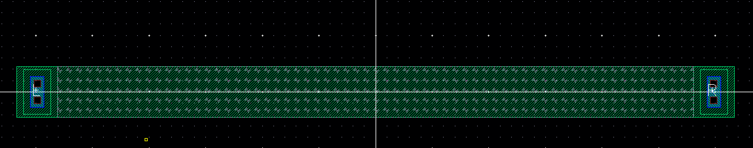
Fig 09: N-well layer resistor with the layer distinguishing it as a resistor and the pins set on the metal1 layer
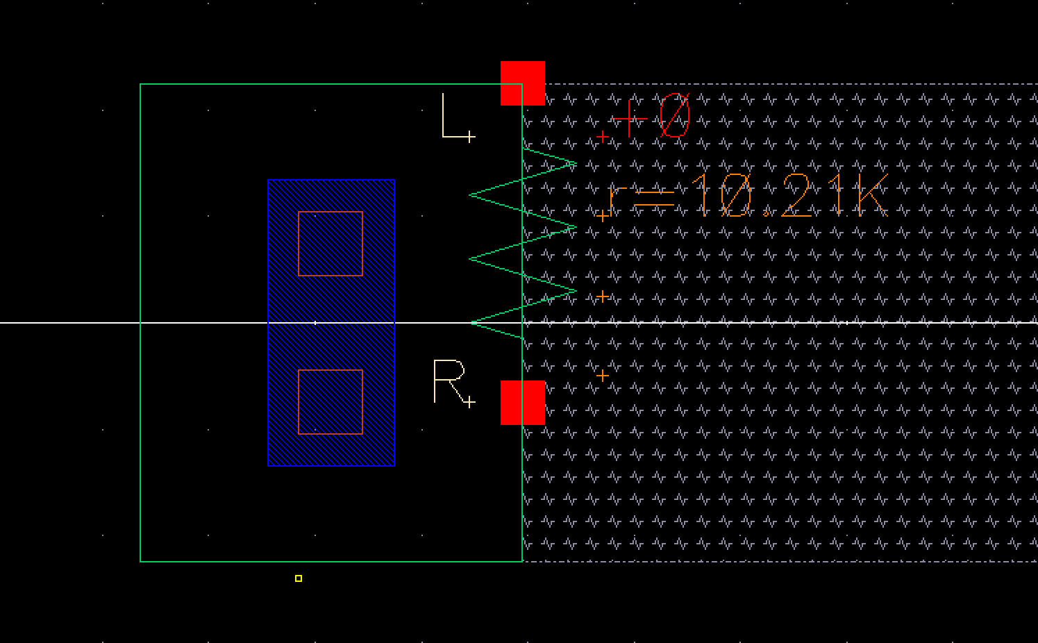
Fig 10: N-well layer resistor extracted file which gives parameter values
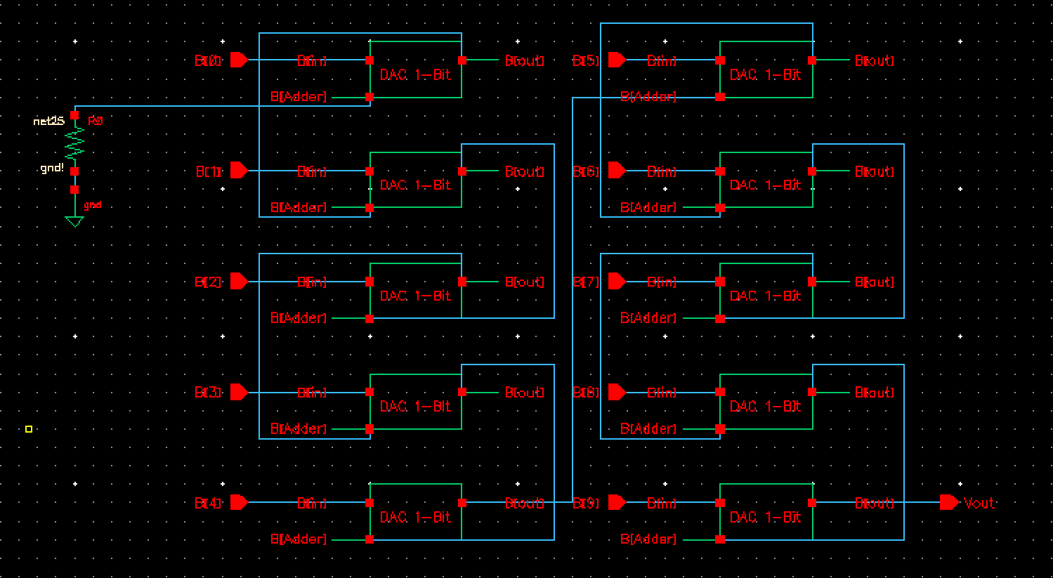
Fig 10: The 10-Bit wired up DAC
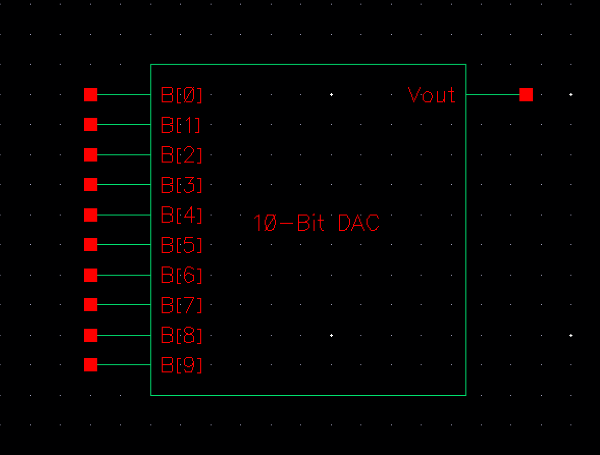
Fig 11: The 10-Bit wired up DAC symbol created
Return to EE 421L labs