Lab 2 - EE 421L
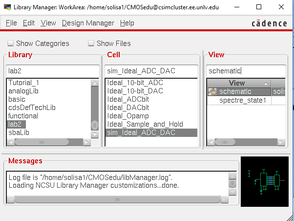
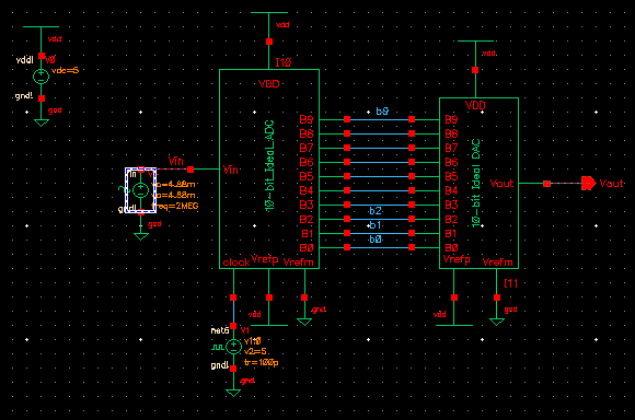
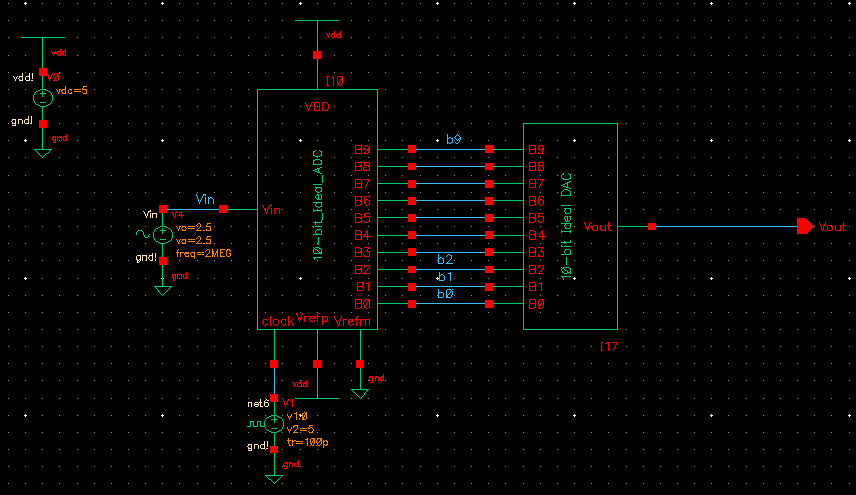
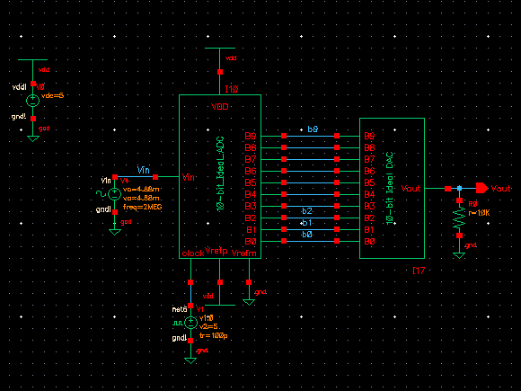
Opening the schematic for the sim_ideal_ADC_DAC as shown below:
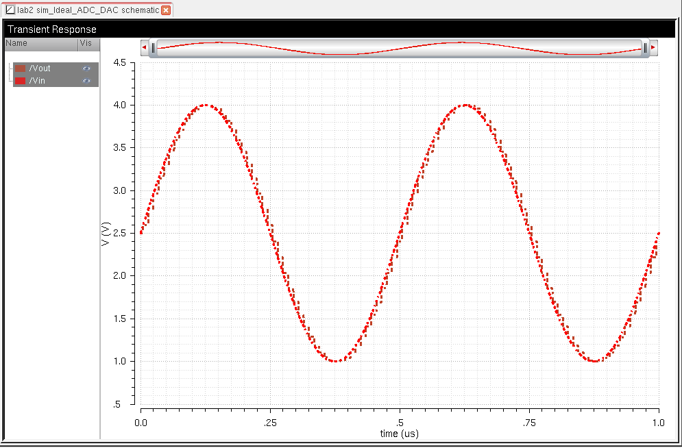
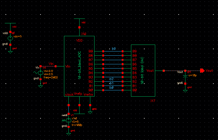
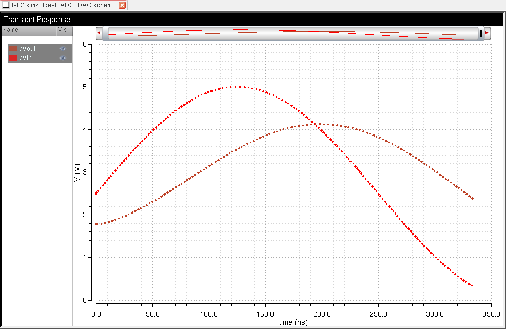
After changing the Vin voltage amplitude to 1.5V gives the following graph:
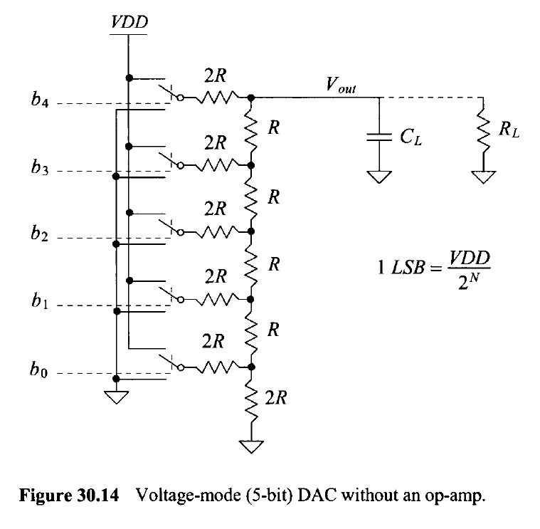
The ADC uses the reference voltage to create a digital signal. The DAC will use the digital signal along with the reference voltage to create an analog signal. The circuit can not use voltages that are higher than 5V or below 0.
Vb0=5V/1024= 4.88mV
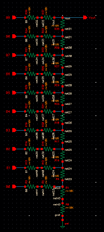
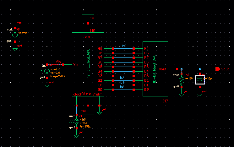
The output resistance of the DAC is R this can be found by combining the resistances in series and parallel in the following fashion:
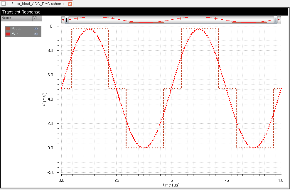
when only b9 is applied a voltage we can expect a waveform like the one below:

When using that R = 10k and C = 10pF we get that .7RC = .7(10*10^3)(10*10^-12) = 70ns.
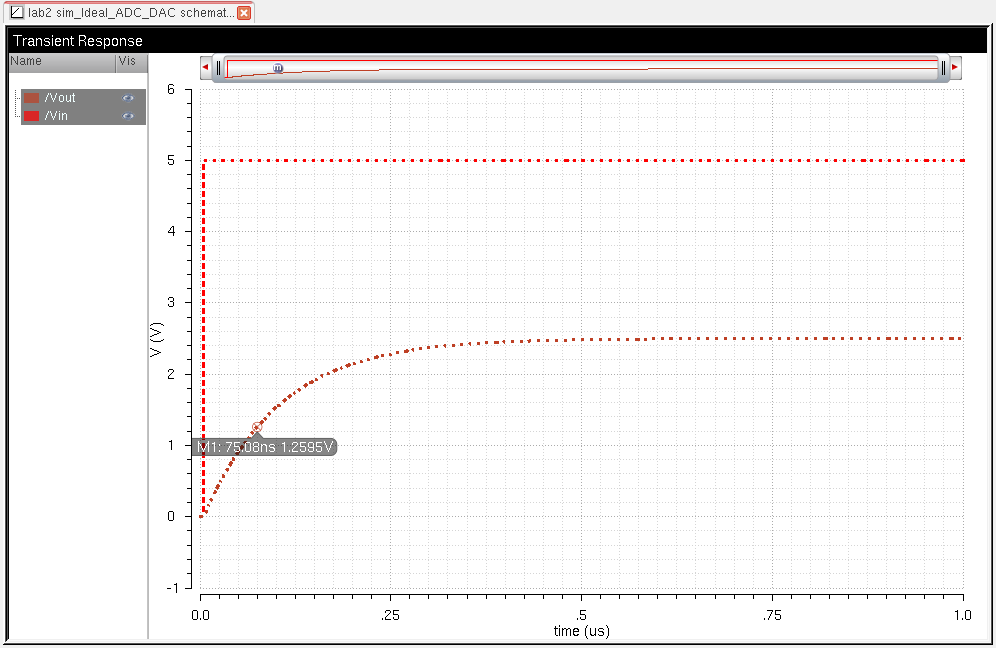
When only B9 is used we can expect the output to be Vin/2. This means that at the .7RC point of 70ns we should see Vin/4 or 1.25V but including our delay of 5ns we get the following:

To create a symbol you must first remove all voltage sources and replace them with input pins. Vout should become an output pin.
Then click Create -> cellview -> from cellview and hit ok.
After replacing the original DAC with our own we get the following output wave:
When adding a 10k resistor load we expect the DAC to act like a voltage divider. And it does because the resistance of the DAC is the same as the load we get half the expected output.

When adding a capacitor of 10pF the output wave begins to have a delay as shown below:
When using both the capacitor and the Resistor we end up with a wave that is both delayed and halved.

If the switch resistance is large when compared to the resistance value used in the DAC then the output voltage will be diminished. This will result in incorrect outputs from the DAC.
My work was backed up via flashdrive and Google Drive.
