Lab 8 - ECE 421L
Authored by:
Brett Smith (smithb25@unlv.nevada.edu)
Aaron Nicolas Escobedo (escoba3@unlv.nevada.edu)
Trevor Ensign (ensigt1@unlv.nevada.edu)
Tuesday, December 5th, 2017
Chip design library for this project: Chip2_f17
For the final lab we were asked to compile a design for a chip to be fabricated. Specifically, the devices to be on the chip are:
- One, or more if possible, course projects (A parity checker)
- A 31-stage ring oscillator with a buffer for driving a 20 pF off-chip load
- NAND and NOR gates using 6/0.6 NMOSs and PMOSs
- An inverter made with a 6/0.6 NMOS and a 12/0.6 PMOS
- Transistors, both PMOS and NMOS, measuring 6u/0.6u where all 4 terminals of each device are connected to bond pads
- Using the 25k resistor laid out below and a 10k resistor implement a voltage divider
- A 25k resistor implemented using the n-well
- Whatever else you would like to fabricate to use the remaining pins on the chip
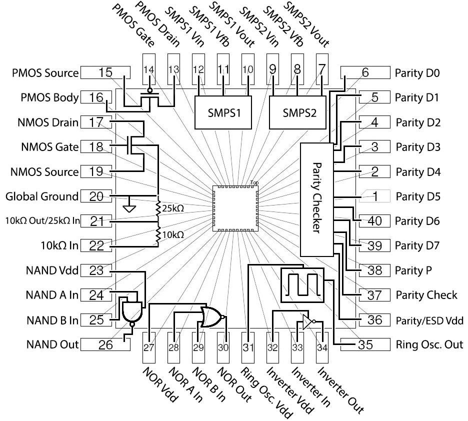
We chose to add two of our SMPS designs from the lecture project to our chip, and that fills up our 40 pins. We chose to lay our chip out using the following chip assignments:
We assembled our chip design and drafted the following schematic and layout:

Schematic |
Layout |

Here are the details of how to use each device on our chip:
Parity Checker:
 |
This even parity checking circuit will output a 1 on the check output when the parity input matches the parity of the input word and will output a 0 when it doesn't match. Pin 36 is connected to the Vdd ESD ring. Only the parity checker is powered by it, but connecting this to Vdd will protect other inputs from high voltage transients. |
||||||||||||||||||||||||||||
Ring Oscillator:
 |
The oscillator will produce a clock signal whenever Vdd and ground are applied with no other stimuli. |
||||||||||
NAND Gate:
 |
|
||||||||||||||
NOR Gate:
 |
|
||||||||||||||
Inverter:
 |
|
||||||||||||
PMOS Device:
 |
|
||||||||||||
NMOS Device:
 |
NOTE: Body connected to pin 20 |
||||||||||
Resistor Divider:
 |
Resistors form a voltage divider if Vdd is applied to pin 22 and ground is connected to pin 20. |
||||||||||
SMPS1:
 |
This is Brett's SMPS design. It requires a .5mH inductor connected between Vout and Vfb and a 1.5uF capacitor connected between Vfb and ground. When connected thos way 3.75V @ up to 100mA output will be produced at the node connected to Vfb. |
||||||||||||
SMPS2:
 |
This is Trevor's SMPS design. It requires a 160uH inductor connected between Vout and Vfb and a 220nF capacitor connected between Vfb and ground. When connected thos way 3.75V @ up to 100mA output will be produced at the node connected to Vfb. |
||||||||||||
The chip DRCs and LVSs and should work as designed once it is fabricated. All data for this project has been backed up in our shared Google Drive folder.

Schematic |
Layout |
