Lab 5 - ECE 421L
Authored by Brett Smith (smithb25@unlv.nevada.edu)
Tuesday, October 10th, 2017
In the prelab for this week the tutorial that I went through was basically the same thing as the lab itself so logic would dictate that completing the lab will demonstrate that I completed the prelab.
For the lab itself I designed two inverters one of size 12u/6u and 48u/24u. The first step was to draw the schematic for each inverter. Because the larger one is the same schematic with a multiplier of 4 this went rather quickly. My schematics can be seen below:
 12u/6u inverter schematic |
 48u/24u inverter schematic |
I then created some simple symbols for each inverter and then got on to laying out the inverters. I laid the MOSFETs out in cell frames as was explained in the book to go along with best practices. This also included a large amount of ntap and ptap devices to allow for better performance at higher currents. My designs are below, as shown they passed DRC and LVS.
 12u/6u inverter symbol |
 48u/24u inverter symbol |
||
 12u/6u inverter layout |
 12u/6u inverter extracted |
 48u/24u inverter layout |
 48u/24u inverter extracted |
 
12u/6u inverter DRC and LVS |
 
48u/24u inverter DRC and LVS |
||
Now that the inverters have been designed it was time to test them. In my simulation I used a variable capacitance and used a parametric analysis with a decade logarithmic step to increase the load from 100fF to 100pF. This allowed me to display all 4 loads on a single graph which makes them easier to compare.
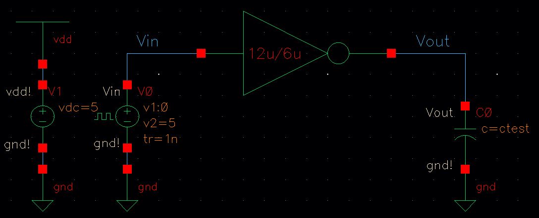 12u/6u inverter simulation schematic |
 12u/6u inverter simulation results |
 48u/24u inverter simulation schematic |
 48u/24u inverter schematic |
Unsurprisingly the larger MOSFET that is effectively providing 4 parallel paths is able to effectively drive a more capacitive load. The striking difference is most visible for the 10pF load where the 48u/24u inverter could potentially be used to drive that load at the speed (not well, but at least it's possible) where for the 12u/6u inverter Vout never goes below Vdd/2 so that inverter never would have shown a transition from high to low for the test impulse.
I messed around with the simulation the extracted model instead of the schematic as well as using UltraSim instead of spectre and saw no difference in my simulation results.
The library for my design can be downloaded here. Both my lab and this website have been backed up.