Lab 4 - ECE 421L
Authored by Brett Smith (smithb25@unlv.nevada.edu)
Tuesday, September 27th, 2017
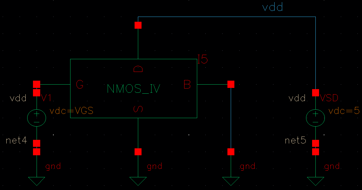
In this lab I drafted an NMOS and a PMOS MOSFET and performed a few simulations on them. To begin with I created copies of the NCSU nmos and pmos cells and performed various simulation to create baseline ID curves.


After I had the basic performance of the devices I placed probe pads on the layout and modified the schematic to match. As you can see on the right I eventually got both design to pass both DRC and LVS.
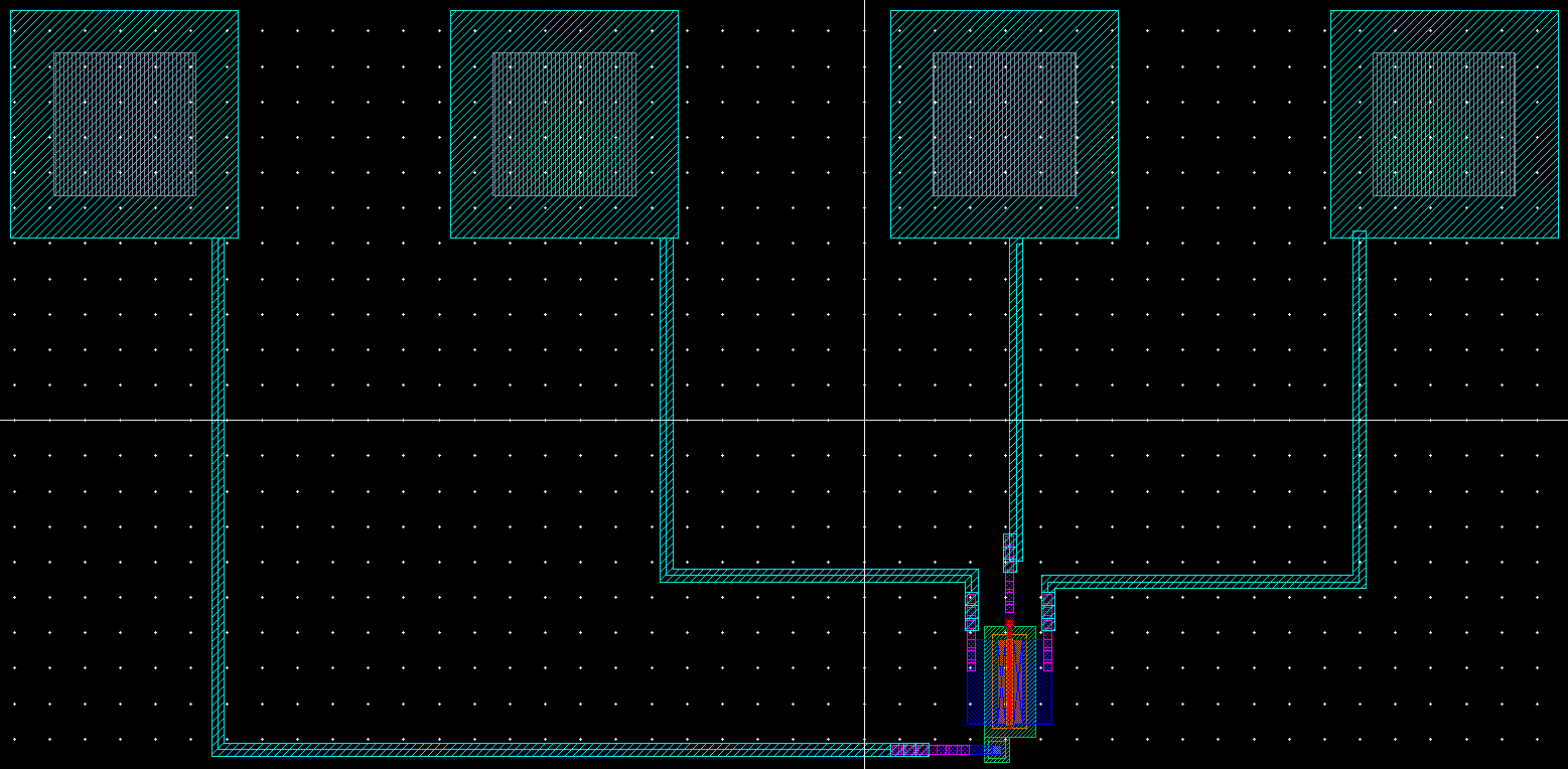
 Layout of my NMOS MOSFET with probe pads  Layout zoomed in to see NMOS device |
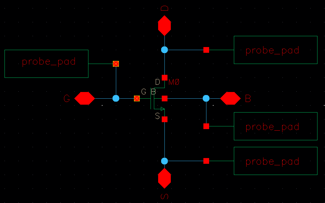 NMOS device schematic  DRC passed  LVS passed |
 Layout of my PMOS MOSFET with probe pads  Layout zoomed in to see PMOS device |
 PMOS device schematic  DRC passed  LVS passed |
Now that my devices could be probed after manufacturing I redid my simulations to ensure that performance had not changed. Below you can see the simulation results that look identical to the previous simulations.


The library for my design can be downloaded here.