Lab 3 - ECE 421L
Authored by Brett Smith (smithb25@unlv.nevada.edu)
Tuesday, September 19th, 2017
In this lab I drafted the layout for the 10-bit digital-to-analog converter (DAC) from the schematic I created in the last lab. This started with designing a 10kΩ n-well resistor that will be used for all of the resistors in the 2R-R resistor ladder. The tutorial suggests to start with a width of 4.5μm by 56μm. Using a sheet resistance of 855Ω/square this should produce a resistor of 855*(56/4.5) = 10.64kΩ. In reality those dimentions doesn't fit onto the layout grid and after adjusting for that it appears that the sheet resistance being used by Cadence is not 855 and is closer to 1.05kΩ/square as this extracted as around a 13kΩ resistor. Massaging the length a bit produced a resistor that was 43.2μm long. This is should produce a resistor of 1.05k*(43.2/4.5) = 10.08kΩ. In terms of the layout scale factor this resistor is 15λ by 144λ. Thinking of it this way allows the same layout to be scaled to any process while maintaining the same resistance provided the new process's sheet resistance is similar to the C5 process that I am designing for. Below you can see the resistor layout and a zoomed in view of the extracted resistor confirming its 10.03kΩ resistance:


Now that a resistor layout with a known resistance has been created I can layout one 2R-R ladder rung that will later be repeated to create the DAC. In the layout below the bit input is on the left, the output (top pin) is the upper piece of metal1 on the right, and the supply from the lower significance bits or ground (bottom pin) is the lower piece of metal1 on the right. The pins themselves are not placed on this layout because they will be placed on the top level layout in the hierarchy.

With the ladder rung designed it is time to put it all together into the larger DAC. Because a modular bit rung has been designed the ladder rungs could be copied any number of times to produce a DAC of any desired resolution, but this assignment asked for 10 bits so I'll go with that. Below you can see a zoomed in view of the two most significant bits, the results from DRC & LVS, and the full DAC layout:
 DAC zoomed view 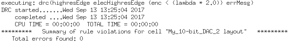 DRC results 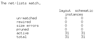 LVS results |
 Full DAC layout |
And that pretty much does it. The library for my design can be downloaded here.