Lab 2 - ECE 421L
Authored by Brett Smith (smithb25@unlv.nevada.edu)
Tuesday, September 13th, 2017
In this lab I will design the schematic for a 10-bit digital-to-analog converter (DAC) using the a resistor ladder construction.
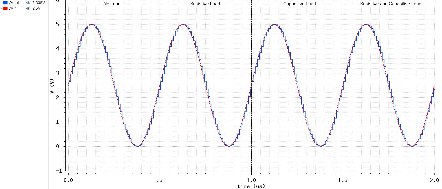
As instructed, for the prelab I downloaded, added to Cadence, and began to look at the lab2 library. In the sim_Ideal_ADC_DAC cell there is an alternating current source that drives the input of an analog-to-digital converter (ADC) with parallel outputs that drive the parallel inputs of the DAC. This causes the sinusoidal input signal from the AC to converted into a stair step output that reasonably approximates the input as shown below:
The stairstep is broken up into 5ns segments while the clock of the ADC is set at 100ps. Handling the ADC as a block box, this is a little confusing as it seems the DAC should be receiving a new setpoint about 50 times more often. If that was the case the stairstep would more closely resemble the AC input signal. I sure this will be explained in time.
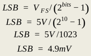
To calculate the least significant bit (LSB) of a DAC the full scale range of the output is divided by the total number of bits minus one (to account for a value of zero). Assuming a full scale range of 5V a 1-bit DAC has an LSB of 5V, a 2-bit DAC has an LSB of 1.67V, and so on. The 10-bit DAC I am to design will have an LSB of 4.9mV when it has a full scale range of 5V as shown by these calculations:
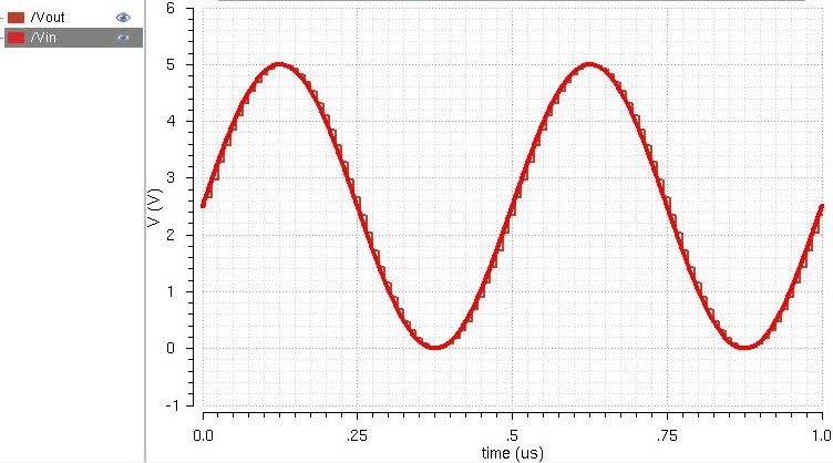
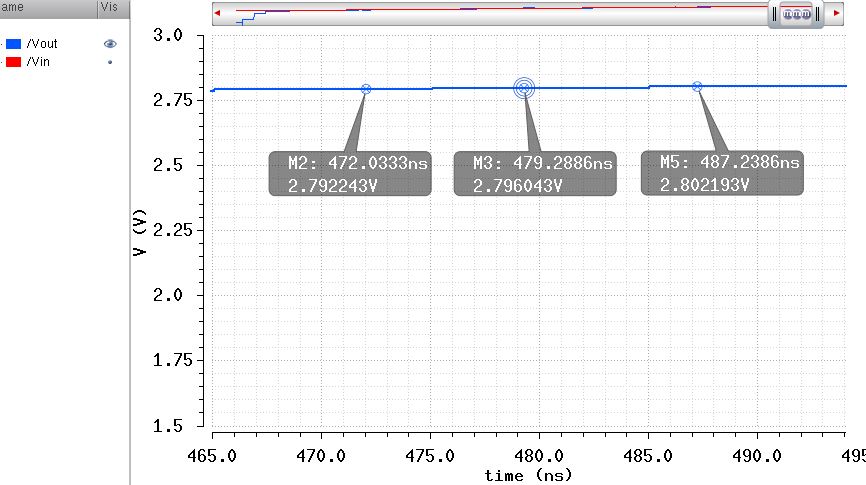
Below is a simulation of the ideal ADC DAC circuit with the frequency of the AC source changed to 40kHz. This slower speed will allow for each step change to be visible on the simulation results. Because the software is trying to simulate physical phenomena the steps are not exactly equal but as you can see below the average of the step changes is 4.98mV which is very close to the calculated LSB.

Moving on to the lab itself, using the examples from the lab document I drafted the schematic to the right (Click for full sized image). As required the 2R segments are built with two separate R resistors in series. I assume this is so when we do the layout for the DAC next week we can create a single 10k resistor model and import that into the DAC layout for all the resistors.
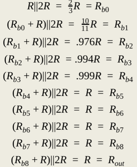
To find the output resistance of the DAC I had to calculate the Thevenin equivalent of the circuit with respect to a load across Vout and ground. Grounding all of the bit inputs this leaves a network of series and parallel resistors. Labeling each node where a 2R resistor meets an R resistor with their respective bit number I found the output resistance of the DAC to be R using the following calculations:
Having calculated the output resistance of 10kΩ, it can be used to calculate the rise time for a step change in the DAC output. Using a capacitive load of 10pF the time for a 50% rise should be .7RC or .7*10kΩ*10pF = 70ns. This result is confirmed in simulation (click either image for full size):
| Circuit Schematic | Simulation Results |
| Circuit Schematic | Simulation Results |
Lastly we were asked to consider the real life situation where the switches controlling each input were replaced with MOSFETs. One of the concerns in this case is if the resistance through the MOSFET is not small compared to R. In that situation it would create a resistor divider between each rung of the carefully constructed resistor ladder and Vdd. This would reduce the source voltage seen by each rung. To make things worse, because each ascending rung has an additional resistor between it and ground the effect would be different for each bit of the DAC. B9 has 12R worth of resistance between it and ground so it will be less susceptible to the MOSFETs resistance causing Vdd drift, but the LSB (B0) only has 3R between it and ground causing the source voltage seen be that rung to drift by 4 times as much as the MSB.