Lab 5 - EE 421L
Authored
by Andy Sam,
sama1@unlv.nevada.edu
10/11/2017
In
lab we, we create CMOS inverter schematics, layouts, and symbols
for sizes 12u/6u and 48u/24u. A CMOS inverter simply consists of a NMOS
and a PMOS wher their respective drain and source are tied together and
both are fed the same input to their gates. Simply it is a switch,
where if the input is high and equal to Vdd, the NMOS transistor is on
and the PMOS is off. This ties the output to ground thus giving a '0'.
If the input is low, the PMOS is on and the NMOS is off. This ties the
output to VDD giving a '1'. After, the designs are tested in SPICE
using both Spectre and then Ultrasim.
12u/6u CMOS Inverter
DRC of 12u/6u CMOS inverter:

LVS of 12u/6u CMOS inverter:

Created symbol of 12u/6u CMOS inverter:

After
designing the symbol, we simulate the 12u/6u inverter using SPICE. The
inverter is tested to a 100fF, 1pF, 10pF, and 100pF capactive load
using Spectre and then Ultrasim.
Signal used to test the inverter:

12u/6u Spectre output with 100fF load:

12u/6u Spectre output with 1pF load:

12u/6u Spectre output with 10pF load:

12u/6u Spectre output with 100pF load:

12u/6u Ultrasim output with 100fF load:

12u/6u Ultrasim output with 1pF load:

12u/6u Ultrasim output with 10pF load:

12u/6u Ultrasim output with 100pF load:

From
all of these simulation, we can conclude that as the capactive load
gets larger, the output signal gets much worse and less sharp. So if we
want a fast switching signal for the CMOS inverter, we should use have
a smaller CMOS load. Also, all results from the Spectre models match the Ultrasim models.
48u/24u CMOS Inverter
DRC of 48u/24u CMOS inverter:

LVS of 48u/24u CMOS inverter:

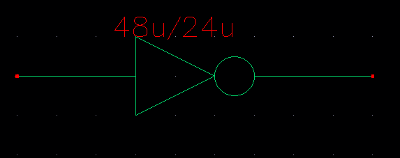
Created symbol of 48u/24u CMOS inverter:
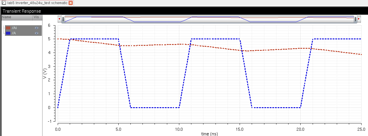
After designing the symbol,
we simulate the 48u/24u inverter using SPICE. The inverter is tested to
a 100fF, 1pF, 10pF, and 100pF capactive load using Spectre and then
Ultrasim.
The same exact signal from the 12u/6u CMOS design is used to test the 48u/24u inverter.
48u/24u Spectre output with 100fF load:

48u/24u Spectre output with 1pF load:

48u/24u Spectre output with 10pF load:

48u/24u Spectre output with 100pF load:
48u/24u Ultrasim output with 100fF load:

48u/24u Ultrasim output with 1pF load:

48u/24u Ultrasim output with 10pF load:

48u/24u Ultrasim output with 100pF load:

The
results are very similar to the 12u/6u inverter. As load capacitence
increases, we get a more delayed and less sharp output signal. But
compared to the 12u/6u inverter, the 48u/24u inverter can take a higher
capacitence load before the accuracy of the output signal drops as
harshly. Once again, the Spectre and Ultrasim models match.
All the cellview files are available here.
Return to EE421 Labs