Lab 4 - EE 421L
Authored
by Andy Sam,
sama1@unlv.nevada.edu
9/20/2017
In
the fourth lab, we analyse PMOS and NMOS schematics for their ID vs V
characteristics. Then we layout the MOSFET devices out in Cadence.
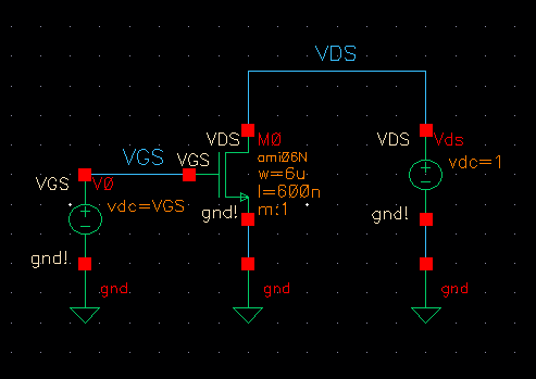
ID vs. VDS of an NMOS device with 6u/600n width-to-length.
VGS varies from 0 to 5V, 1V steps. VDS varies from 0to 5V, 1mV steps.

ID vs. VGS of an NMOS device with 6u/600n width-to-length.
VGS varies from 0 to 2V, 1mV steps. VDS = 100mv.


ID vs. VSD of an PMOS device with 6u/600n width-to-length.
VSG varies from 0 to 5V, 1V steps. VSD varies from 0 to 5V, 1mV steps.


ID vs. VGS of an PMOS device with 6u/600n width-to-length.
VSG varies from 0 to 2V, 1mV steps. VSD = 100mV.


Layout of NMOS device:
DRC:

Schematic:

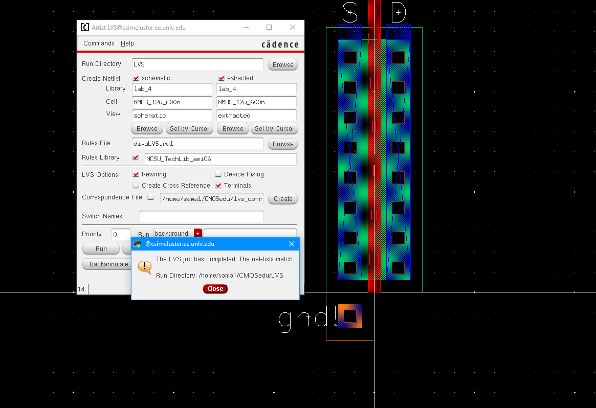
LVS:
Layout of PMOS device:
DRC:

Schematic:

LVS:

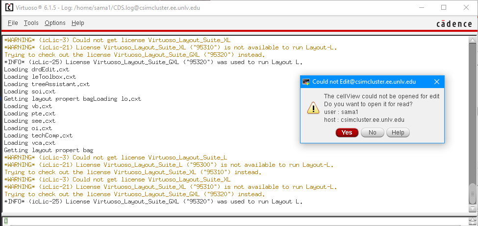
Error note:
Just as I was doing the pad layouts for the NMOS and PMOS, Cadence crashed and locked out my layout files.

As
I attempted to open them, I got the following error and could not
figure out how to unlock these files. As such, the above layouts were
snipped before pads were added. Could the grader explain how to fix
such error in the return email?
Return to EE421 Labs