Lab 3 - EE 421L
Authored
by Andy Sam,
sama1@unlv.nevada.edu
9/13/2017
In the third lab, we take the design of the DAC from the second lab, and then create layout of it.
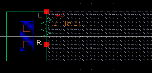
The first thing we do before laying out the actual DAC is layout its main part, a 10k ohm resistor. Just like in Tutorial 1,
we
layout a 10k ohm resistor. The width and length of the n-well are
selected based on the resistance we need and are constrainted by
parameters in the MOSIS process. First, we are constrained by a minimum
n-well width of 12 lambda. In our case, lambda is 300nm, so we are
constrained with a minimum 3.6um width. Second, the sheet resistance in
the C5 process is roughly 800ohms/um^2. Third, everything must snap to
0.15um. With these constraints, we decided on a length of 56.1um and a
width of 4.5um. This is not exact as the 0.15um snap restricts us, and
sheet resistance is not exactly 800.


Using DRC to verify, we get no errors. After extracting the n-well resistor, we also get the exact resistance of 10.21k ohms.
After we layout the single resistor, an R2R version of it to easily copy over the DAC design.

Finally, we layout the entire R2R DAC completely vertically. All pin connections are done by metal1.
Every
resistor is laid out perfectly vertically thanks to the copy tool
(shortcut C). The copy tool has an option to snap the copied object
vertically, horizontally, orthangonally, etc. By snapping it vertically
and creating many instances, a 10 bit DAC is created very quickly and
neatly.

To
measure distance between each resistor to ensure they are not too close
and to measure the width and lengths of the resistors, we can easily
use the ruler tool (shortcut K). This will ensure we have proper
distance between each resistor and correct size. After we get the first
resistor set correct, the copy tool should handle the rest.

After the layout, we verify the layout design using DRC. There were not errors in the DRC check.


Finally, the layout is extracted and now usable for future projects that require the 10-bit DAC.

Return to EE421 Labs
