
Lab 2 - EE 421L


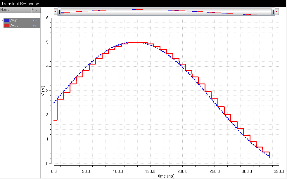
Finally, a transient reponse is ran under 1us by going to Launch ADE, loading the cellview state, and then starting the simulation. From the figure below, we can see that Vin is a straight sin wave, while Vout is a jagged sign wave that looks like many little steps instead.


| ON(5V) | B1 | B3 | B4 | B7 | B8 |
| OFF(0V) | B0 | B2 | B5 | B6 | B9 |
To analyze a different DC signal, a 1V source was used instead. We can easily see the ADC output signals change in the graph. instead, we get a signal with all the outputs shifted over by 1 digit. Starting with B9, the signal is shifted from 0110011010 to 0011001101. Because we went from 2V to 1V, this makes absolute sense as shifting right by 1 digit is the same as dividing by 2 in digital logic.

| ON(5V) | B0 | B2 | B3 | B6 | B7 |
| OFF(0V) | B1 | B4 | B5 | B8 | B9 |
3)
Based on the DC simulations done in the previous step, it is certain
that B0 is the least significant bit. The reasoning is because we took
a 2V signal and turned it to a 1V signal, we divided the signal by 2.
By dividing an analog signal by 2, the digital signal should also be
divided by 2. A digital signal divided by 2 means that the bits of the
signal were right shifted by 1. If we assume B9 is the LSB, we go
from 0101100110 to 1011001100. This is clearly NOT a right shift by 1.
If we assumed B0 as the LSB, we go from 0110011010 to 0011001101. This
is a right shift by one. So in conclusion, B0 is the LSB.
Postlab
The 10-bit DAC is designed using an R2R ladder with 10k ohm resistors.

Here is the ladder in detail. For the first bit (B0), we have 2R in parallel with 2R where R = 10k ohms. Every bit after that is 2R followed by R.

To determine the output resistance of the DAC, we can create Thevenin equivalent circuits from the large circuit. First divide out each R2R section of the circuit. For the first portion (B0), we will have 2R parallel with 2R. 2R parallel with 2R simplifies to R.


Next, we have the B1 section. Because B0 simplified to R, B1 is R in series with R, which is then in parallel to 2R. R in series with R turns into 2R. Once again, we have 2R parallel with 2R which simplifies to R.

From here, it is just a constant repeat of R in series with R, which is then parallel with 2R. The final result will be an output resistance of R which is 10k ohms in our case.
When B0-B8 are grounded, and B9 is give a pulse (0 to VDD), we can predict the delay of the DAC given a 10pF load using 0.7RC. The delay should be the following:

If we include the 10ns delay before the input hits its 5V peak, at 70ns delay (80ns real time), we can see the voltage of the output is at roughly 1.3V. The actual 63.2% of 2.5V is 1.5V, but we are very close to the actual value.

To create a symbol from the schematic, simply do the following. First add pins to your schematic. Pins will determine your inputs, outputs, and bidirectionals. After so, go to Create -> Cellview -> From Cellview. Once the popup menu comes up, you can hit okay. In the next menu, you will determine where your pins will go in the block diagram. Select where each pin will go, and then hit OK. After that, your schematic symbol will be created and can be used in other schematics. The following picture is an example of a created symbol using my_DAC design:

After creating the symbol, the DAC in the original LAB2 file is replaced by my_DAC and tested out.

When simulating no load, the simulation works as expected. It creates the same staircase like output we saw in the prelab that tries to match up the the sine wave of the input voltage.
In the case of a resistive load of 10k ohms, we get half of the input voltage but in the same staircase like output. This makes sense as the output resistance of the R2R DAC is 10k ohms. When put in parallel with a 10k ohms load, we should get a voltage divider that divides the voltage by 2 (as a voltage divider with both resistors being equal divides voltage by 2).

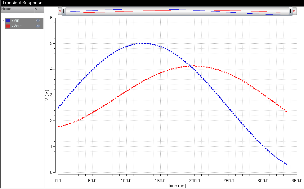
With a 10pF capacitive load, we get a delay of roughly 70 nanoseconds from the peak of the input to the peak of the output. We also lose some output voltage, but there is no staircase like jagged wave. The output wave smooths out to be like a sine wave.
With an RC load of 10kohms and 10pF, we experience both a delay in the wave, a great loss of output voltage, and a smoother sine wave. This makes sense as the 10k resistor roughly divided the output voltage by 2. The capacitor itself added a delay and a smooth sine wave. Combined, we should get similar results, but do note the delay is shorter in this RC load. This is probably because the output voltage combined with the load voltage in parallel creates a smaller total R than either alone. As 0.7RC is linear, a smaller overall R gives us a smaller delay.
