EE 421L: Digital Integrated Circuit Design Lab
Project
Prachi Patel
patelp3@unlv.nevada.edu
Parity Checker
Schematic due: Nov 15, 2017
For
our project, we are designing a parity checker that outputs 0 when the
number of 1 in a 9-bit input is odd and 1 when it is even. Since the
putput is "valid" when the input has even number of 1's, the parity
checker is also called an even parity checker. For the first part of our poject, we design the schematic for this parity checker.
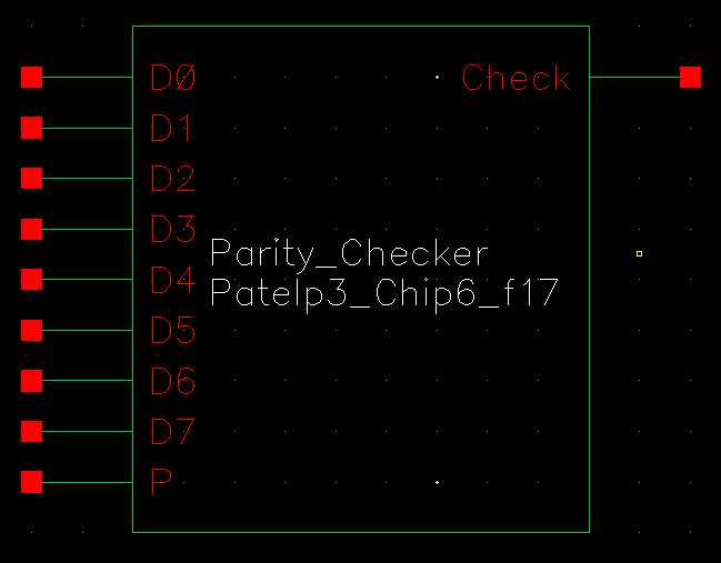
There
are 9-bits of inputs, D0-D7 is eight of them and the P, parity, is the
ninth input. D0-D7 are inputs from 2-bit XOR gates that we created for
previous labs. The XOR gates work in the following way for 2-bit:
D0
|
D1
|
Output
|
0
|
0
|
1
|
0
|
1
|
0
|
1
|
0
|
0
|
1
|
1
|
1
|
If there are even number of 1 (or high) inputs (i.e. 0,2,4,6...), the
output is 1, and if there are odd number of 1 in inputs (1,3,5...), the
output is 0.
Below is the schematic for the parity checker. The first 8-bit input
output an even or odd logic and if that output matches the parity P,
the Check is high (valid), and if it doesn't, the check is low
(invalid). The inverter added at the end is used as a buffer.
This inverter helps us count the even parity as 9-bit and outputs 0
(invalid) when the total number of 1's is odd and 1 when even.

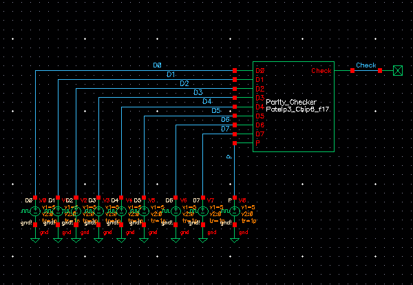
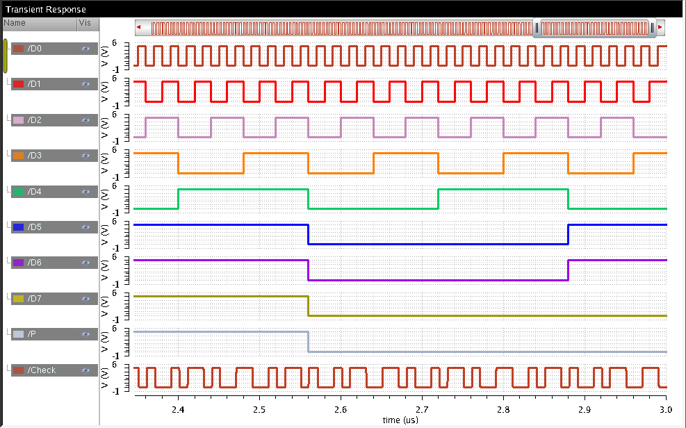
The schematic was converted into a symbol as seen below for ease of
simulation and comprehension. Each input has different pulse width and
time period to gain check with every possible combination of 9-inputs
(2^9 = 512 combinations!)
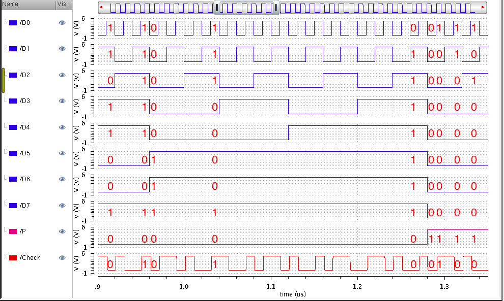
A we see below, I added some examples.
- For the first one, the first 8 inputs, D0-D7 has 5 inputs of 1's,
which is odd so the output from D0-D7 will be 0. The parity P is 0, so
the number of 1 remain 5, an odd number. So the check is 0.
- The second one has 6 (even) 1's, but the parity is 0, which keeps
the total number of 1's in the logic as even, so the output is 1.
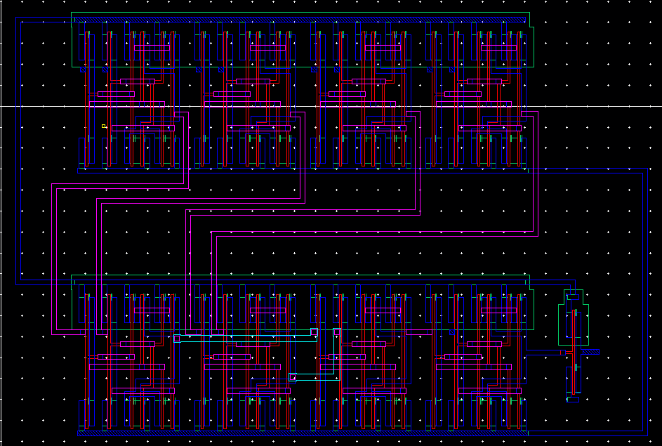
Layout
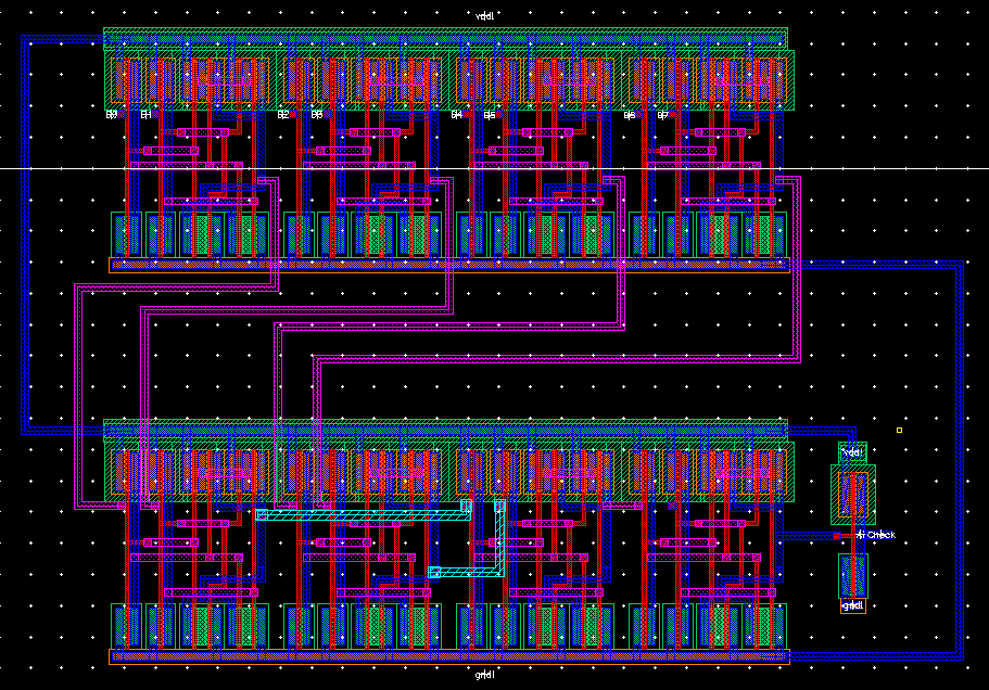
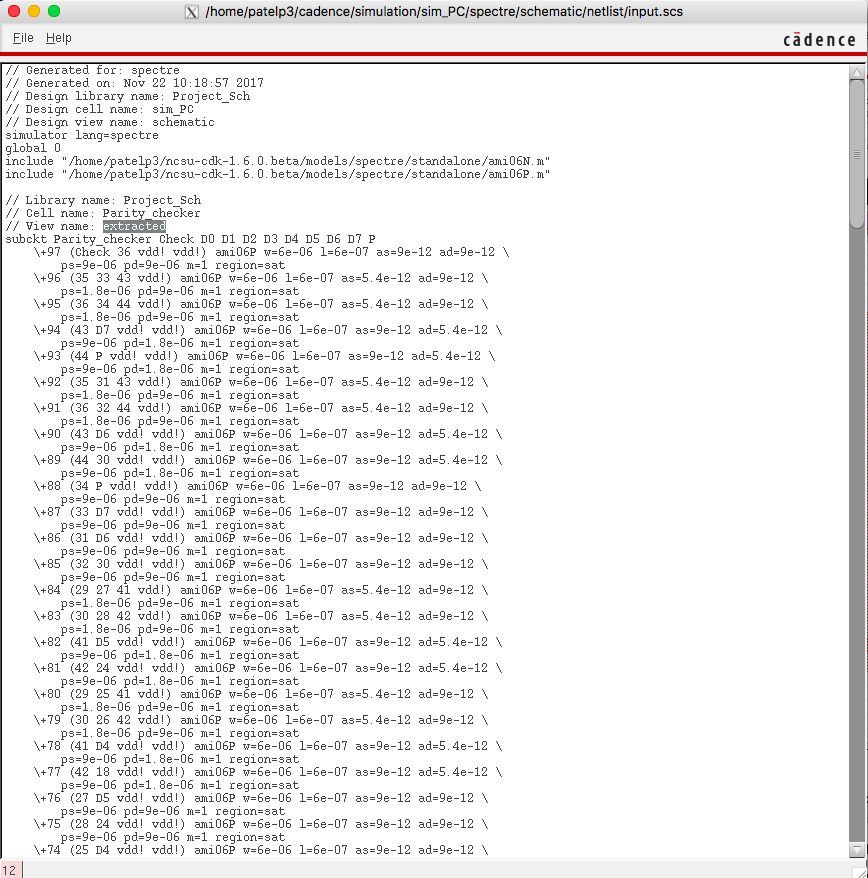
Extracted
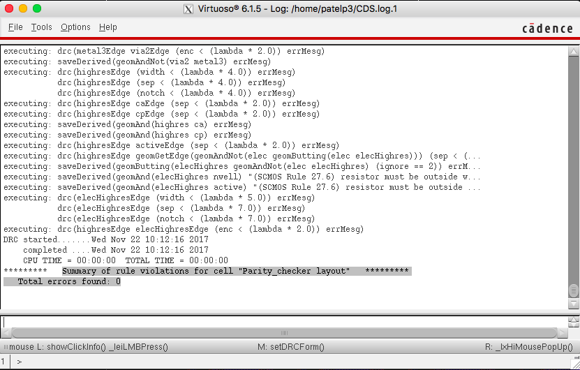
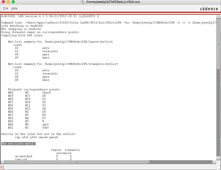
DRC / LVS
Schematic files: Project_Sch.zip
Return to labs