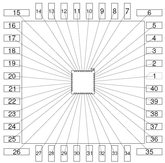
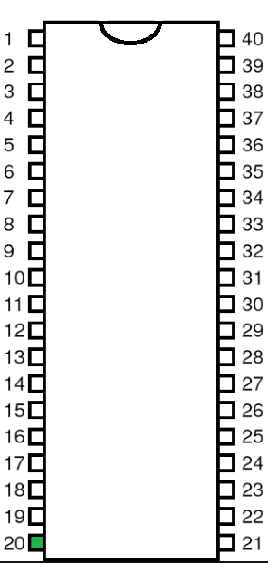
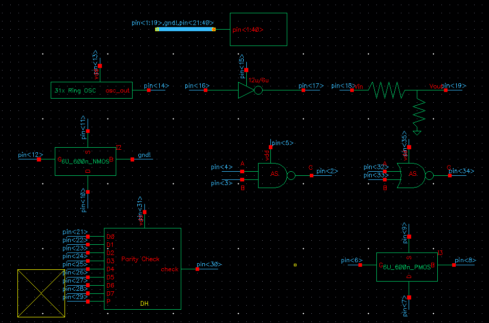
Complete Pin Table
| Pin |
Device |
Connection |
Pin |
Device |
Connection |
Pin |
Device |
Connection |
Pin |
Device |
Connection |
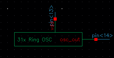
| 1 |
13 |
Ring Oscillator |
Vdd |
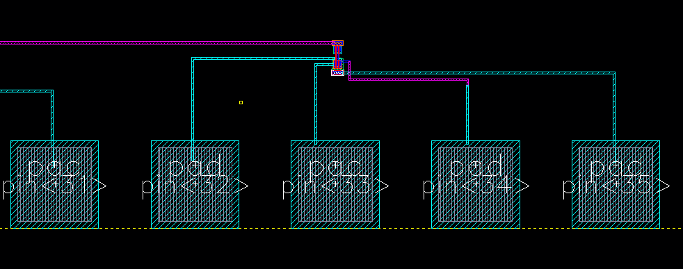
25 |
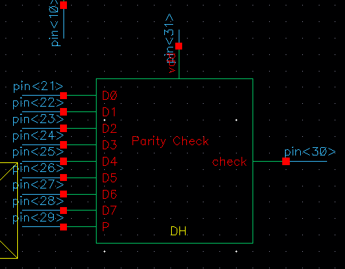
Parity Checker | D4 |
37 |
||||
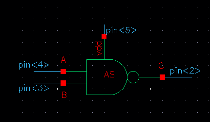
| 2 |
NAND |
C |
14 |
Ring Oscillator |
out |
26 |
Parity Checker | D5 |
38 |
||
| 3 |
NAND |
B |
15 |
Inverter |
Vdd |
27 |
Parity Checker | D6 |
39 |
||
| 4 |
NAND |
A |
16 |
Inverter |
A |
28 |
Parity Checker | D7 |
40 |
||
| 5 |
NAND |
Vdd |
17 |
Inverter |
Ai |
29 |
Parity Checker | Parity |
|||
| 6 |
PMOS |
Gate - G |
18 |
Voltage Divider |
Vin |
30 |
Parity Checker | check |
|||
| 7 |
PMOS |
Drain - D |
19 |
Voltage Divider |
Vout |
31 |
Parity Checker | Vdd |
|||
| 8 |
PMOS |
Body - B |
20 |
Common |
GND! |
32 |
NOR |
A |
|||
| 9 |
PMOS |
Source - S |
21 |
Parity Checker |
D0 |
33 |
NOR |
B |
|||
| 10 |
NMOS |
Drain - D |
22 |
Parity Checker | D1 |
34 |
NOR |
C |
|||
| 11 |
NMOS |
Source - S |
23 |
Parity Checker | D2 |
35 |
NOR |
Vdd |
|||
| 12 |
NMOS |
Gate - G |
24 |
Parity Checker | D3 |
36 |
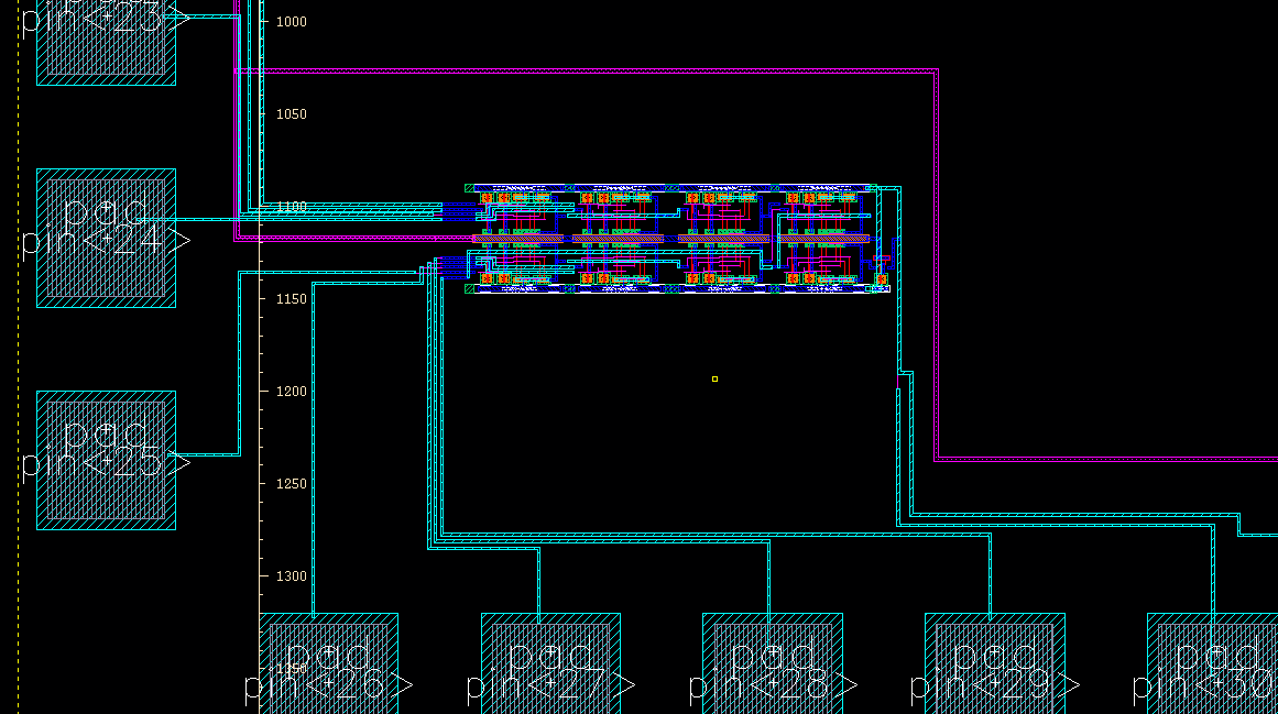
| Schematic |
 |
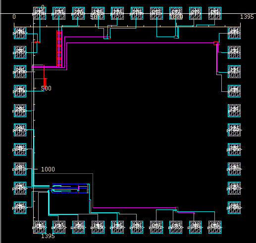
| Layout |
 |
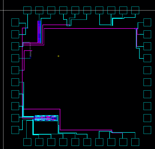
| Extracted |
 |
| DRC |
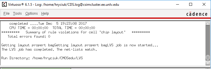 |
| LVS |
 |
| Pin |
Device | Connection |
| 20 |
Common |
GND! |
| 21 |
Parity Checker |
Input - D0 |
| 22 |
Parity Checker |
Input - D1 |
| 23 |
Parity Checker | Input - D2 |
| 24 |
Parity Checker | Input - D3 |
| 25 |
Parity Checker | Input - D4 |
| 26 |
Parity Checker | Input - D5 |
| 27 |
Parity Checker | Input - D6 |
| 28 |
Parity Checker | Input - D7 |
| 29 |
Parity Checker | Input - Parity |
| 30 |
Parity Checker | Output - Check |
| 31 |
Parity Checker | Input - Vdd |
| Pin |
Device |
Connection |
| 2 |
NAND |
Output - C |
| 3 |
NAND |
Input - B |
| 4 |
NAND |
Input - A |
| 5 |
NAND |
Input -Vdd |
| 20 |
NAND |
Common - GND! |
| Pin |
Device |
Connection |
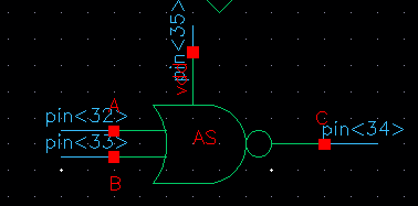
| 32 |
NOR |
Input -A |
| 33 |
NOR |
Input - B |
| 34 |
NOR |
Output - C |
| 35 |
NOR |
Input - Vdd |
| 20 |
NOR |
Common - GND! |
| Pin |
Device |
Connection |
| 13 |
Ring Oscillator |
Input - Vdd |
| 14 |
Ring Oscillator |
Output - out |
| 20 |
Ring Oscillator |
Common - GND! |
| Pin |
Device |
Connection |
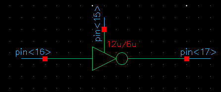
| 15 |
Inverter |
Input - Vdd |
| 16 |
Inverter |
Input - A |
| 17 |
Inverter |
Output - Ai |
| Pin |
Device |
Connection |
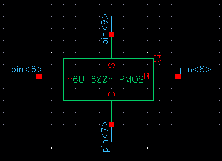
| 6 |
PMOS |
Gate - G |
| 7 |
PMOS |
Drain - D |
| 8 |
PMOS |
Body - B |
| 9 |
PMOS |
Source - S |
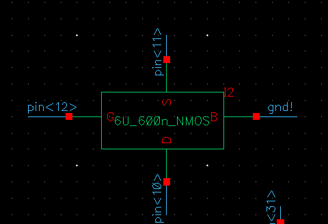
| Pin |
Device |
Connection |
| 10 |
NMOS |
Drain - D |
| 11 |
NMOS |
Source - S |
| 12 |
NMOS |
Gate - G |
| 20 |
NMOS |
Body - B (Common - GND!) |
| Pin |
Device |
Connection |
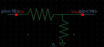
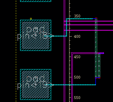
| 18 |
Voltage Divider (25K) |
Input - Vin |
| 19 |
Voltage Divider |
Output - Vout |
| 20 |
Voltage Divider (10K) |
Common - GND! |