LAB 7 - EE 421L
Prachi Patel
patelp3@unlv.nevada.edu
PRELAB:
I updated files to Google Drive.
The ring oscillator created is as shown below in the lab. I used the same one and changed the size from <0:30> to <0:4>.
LAB:
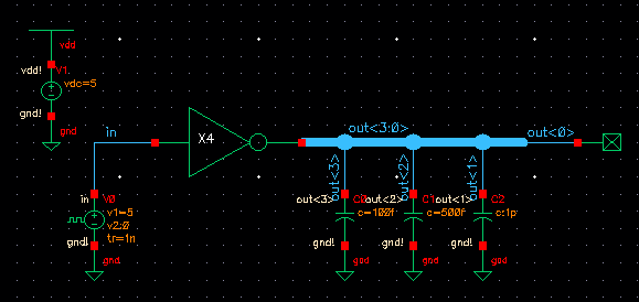
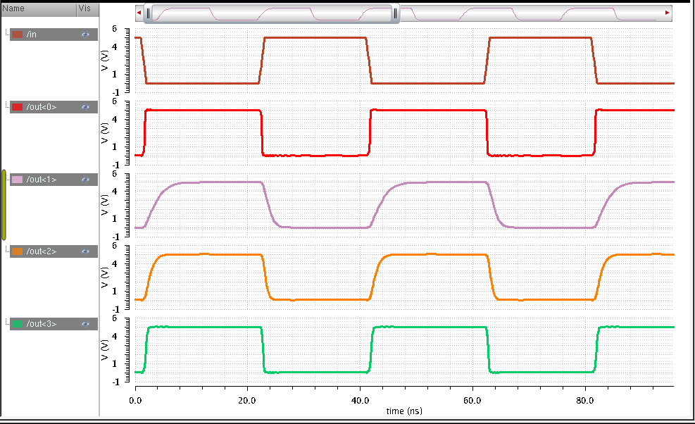
The following 4-bit inverter uses bus wire to create an array of
4-inverters. I turned that schematic into a symbol of x4 inverter and
then simulated it using three different capacitors and pulsing voltage
source.
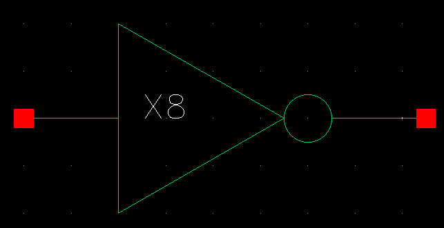
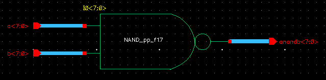
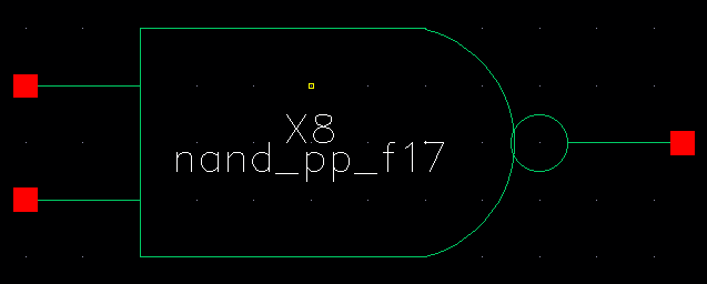
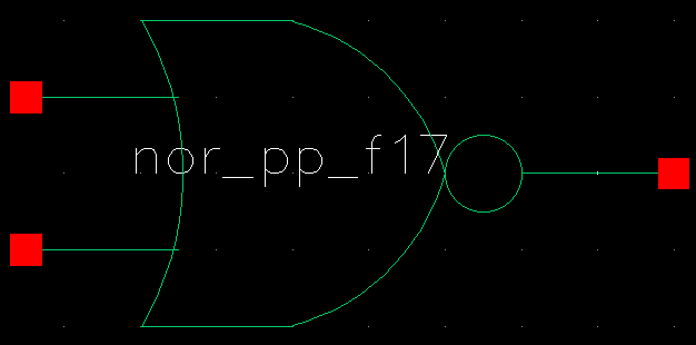
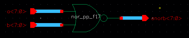
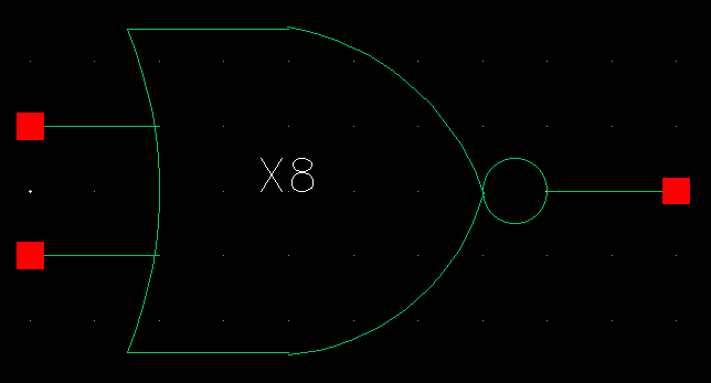
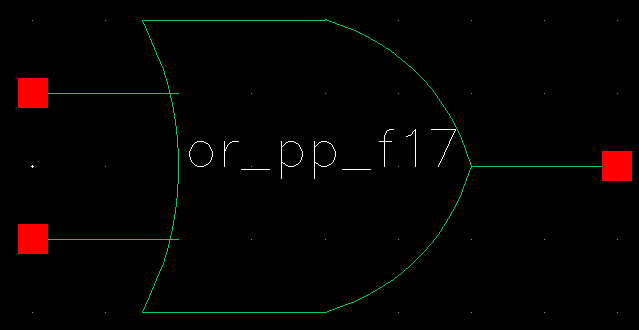
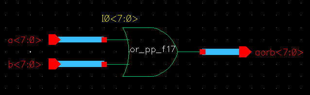
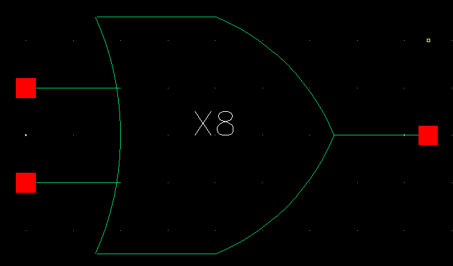
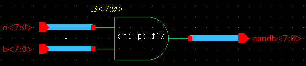
INVERTER, NAND, NOR, OR and AND Gates
The NAND and Inverter were already created
previously so I used the symbols to create a 8-bit ring-oscillator. For
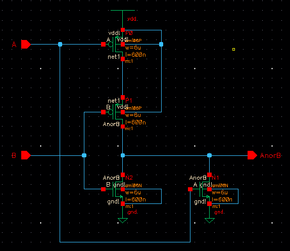
NOR, OR and AND, I used the schematics developed below to create 1-bit
symbols and then created the 8-bit ones.
For simulations, I used an example from one of the previous labs and
simulated them all at once using capacitors of load 100f, 500f, and 1p
F.
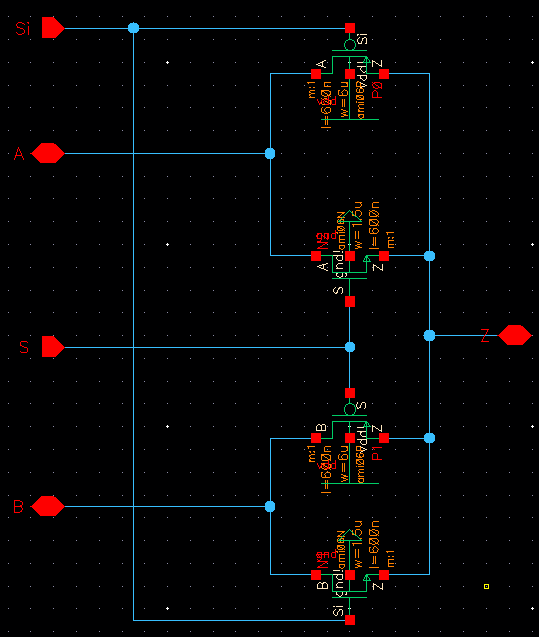
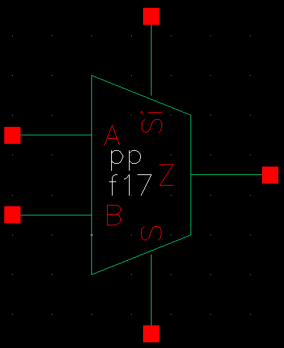
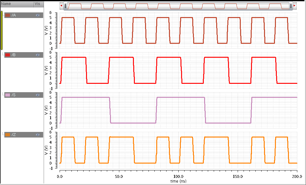
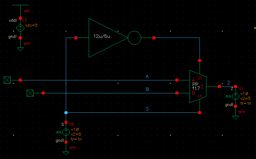
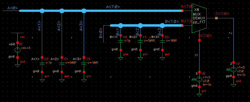
Next, I used the given schematic to create MUX/DEMUX.
Here, A B and Z are inputoutput while Si, S are inputs. This way, the
schematic can work as MUX and DEMUX by changing sources and loads.
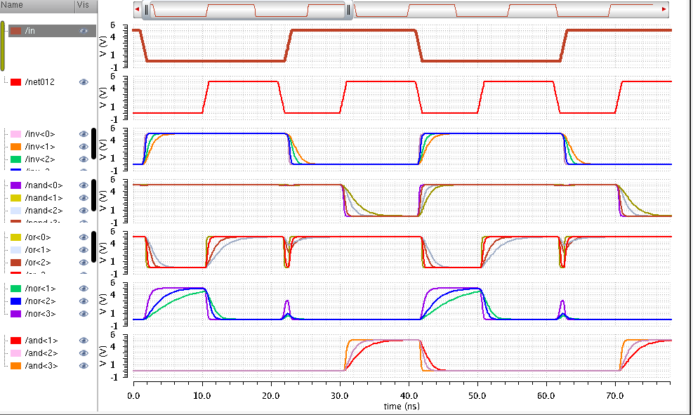
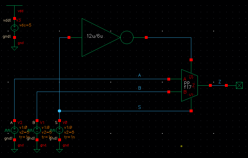
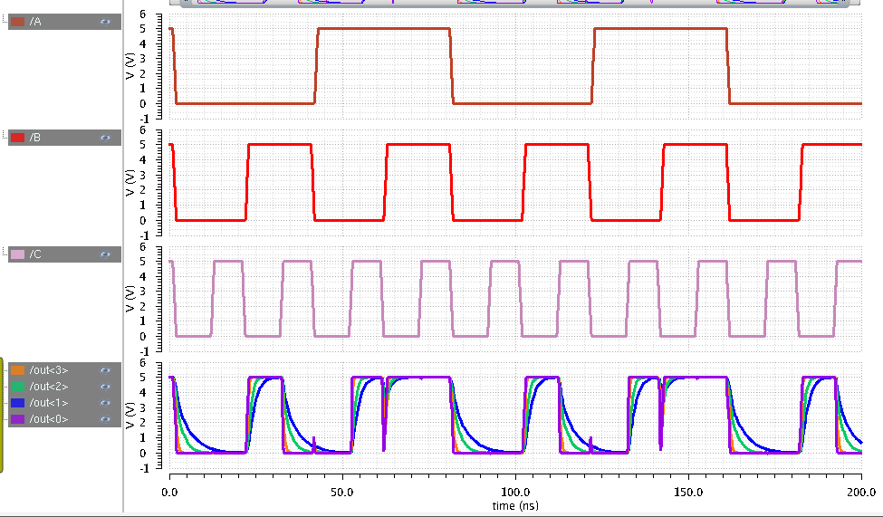
The following are simulations for MUX, where A, B and S are inputs.
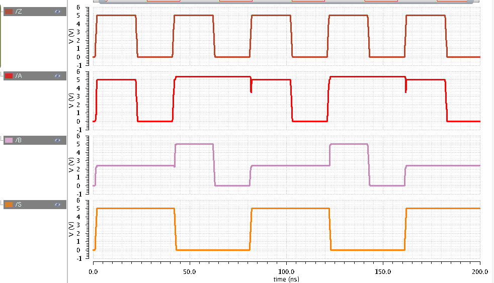
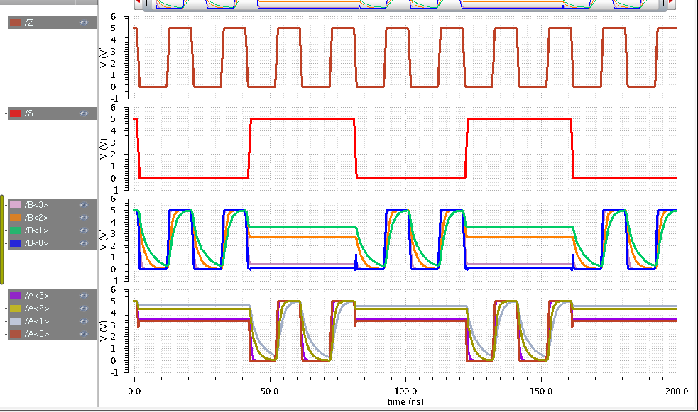
This is the simulation for DEMUX where Z and S are inputs.
The following simulation is for Mux, using 8-bit MUX.
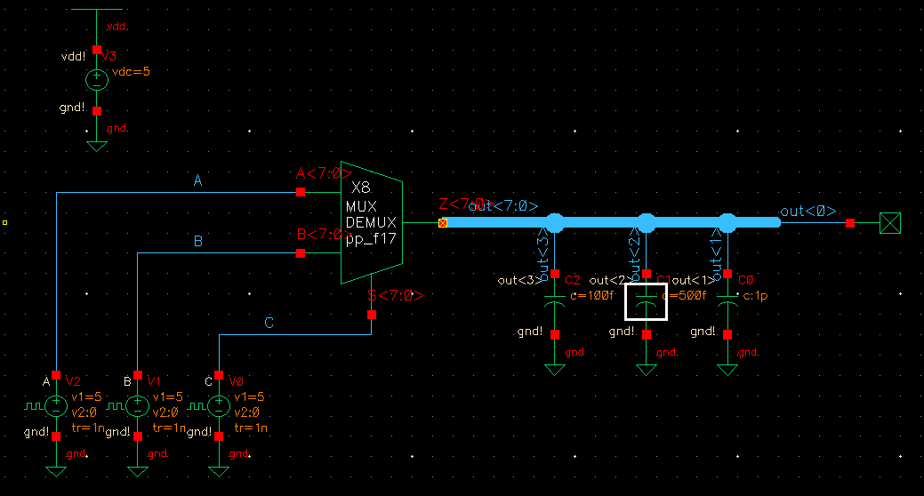
This simulation is for Demux, using 8-bit MUX/DEMUX.
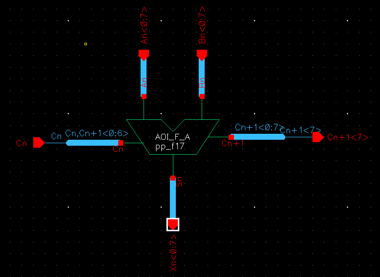
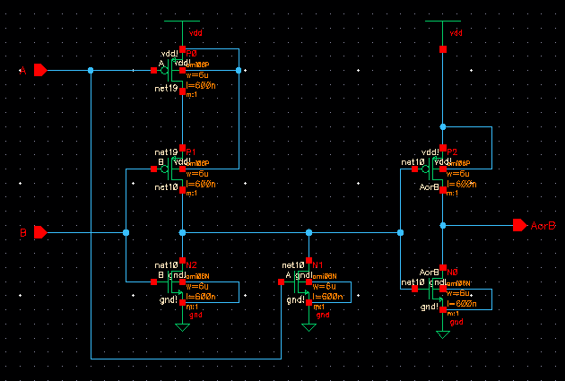
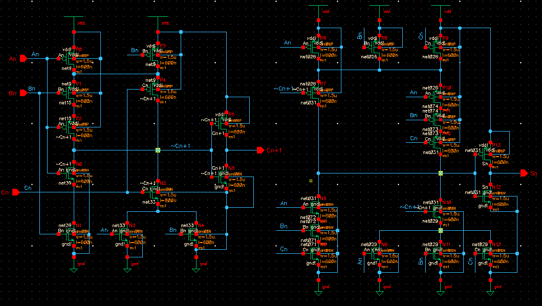
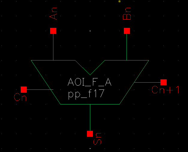
Next, I creates AOI Full Adder schematic using the book. Instead of
symbols like inverter, I used PMOS and NMOS to better figure out the
layout later.
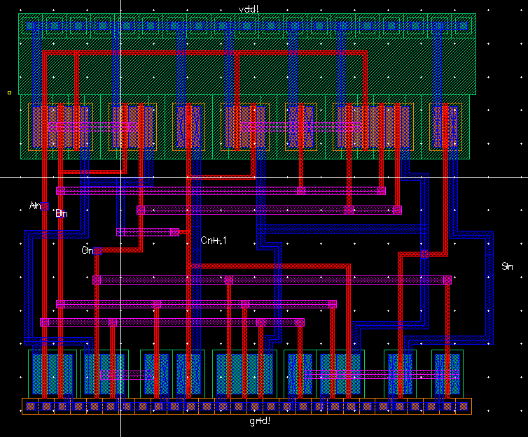
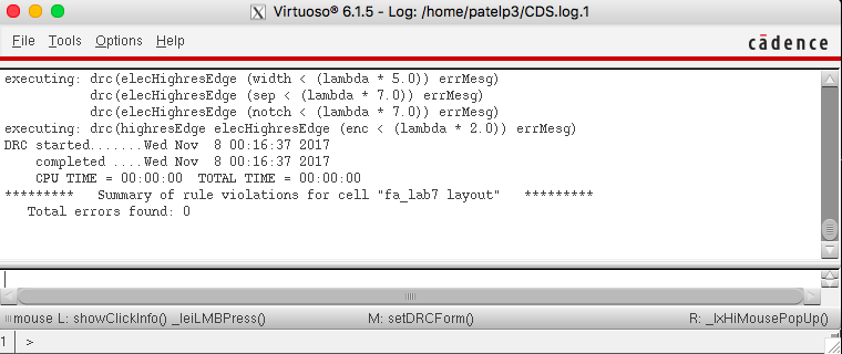
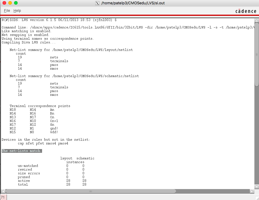
Next, I converter the schematic into a symbol and then layout. The
following images include schematic, symbol, layout, DRC, extracted and
LVS of the AOI Full Adder.
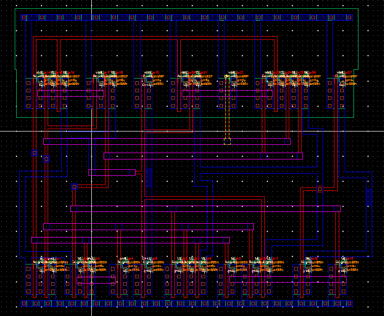
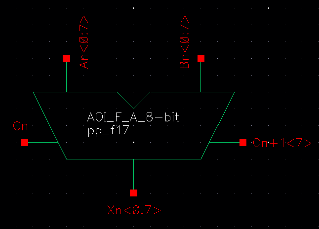
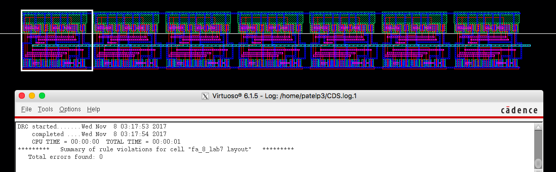
This is similar to above, except it's an 8-bit AOI Full Adder. The following includes Schematic, Symbol, Layout, DRC and LVS.