LAB 6 - EE 421L
Prachi Patel
patelp3@unlv.nevada.edu
October 25, 2017
Prelab:
Tutorial 4 where we created Nand Gate. (Pictures in the lab below).
Uploaded all the work to Google Drive.
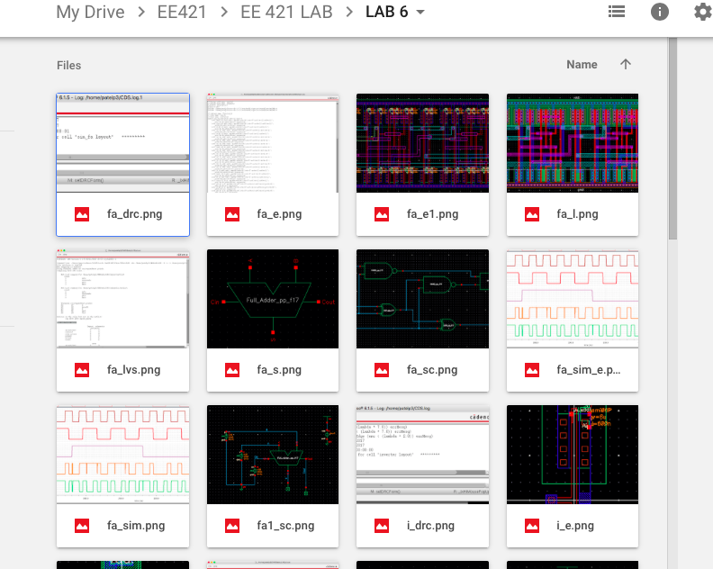
LAB:
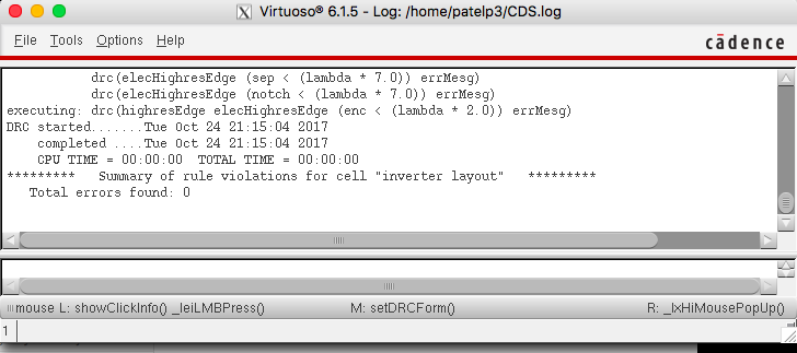
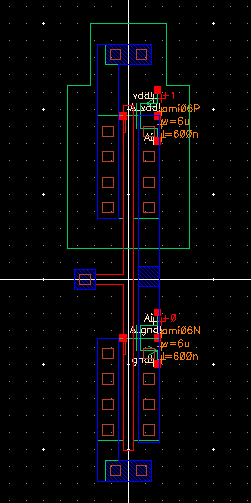
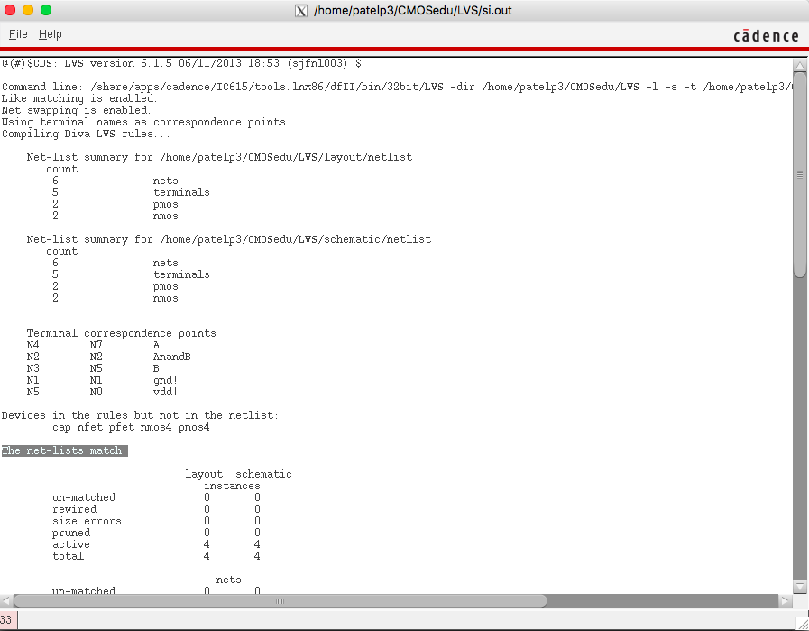
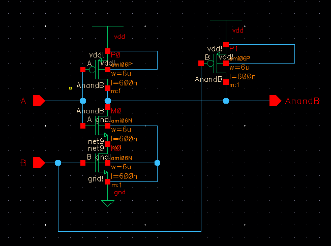
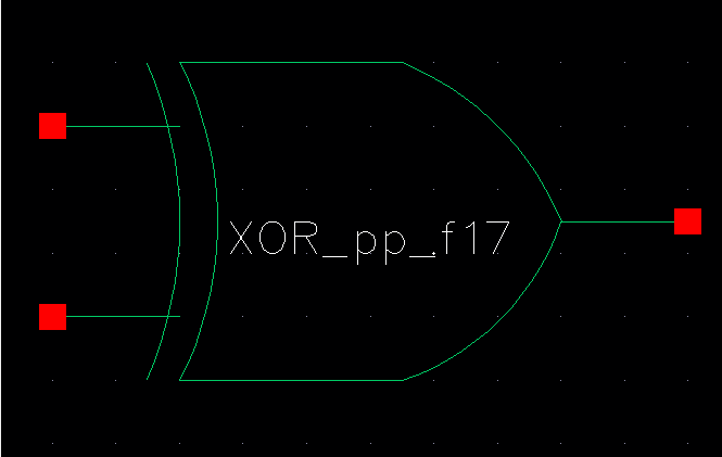
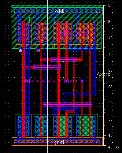
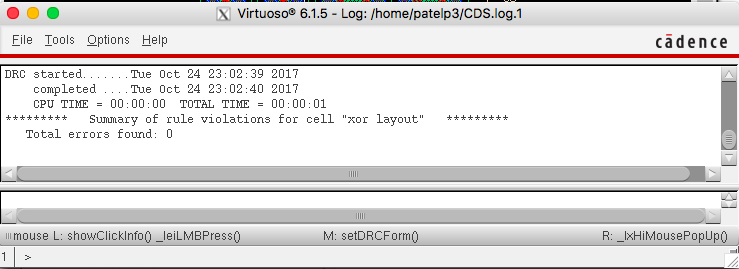
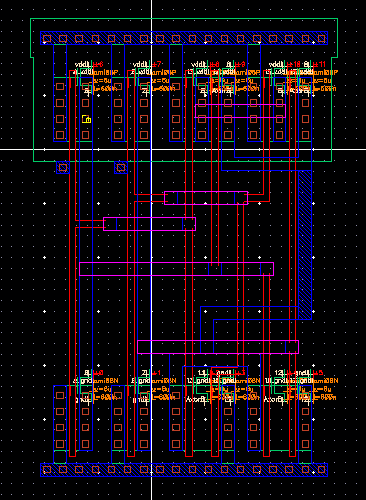
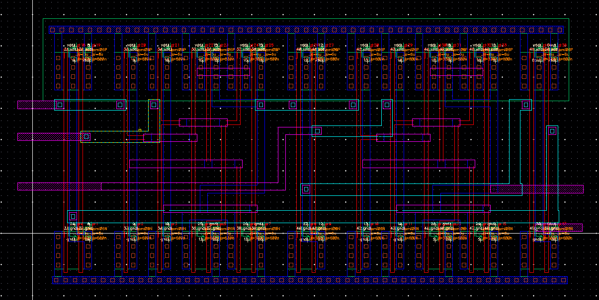
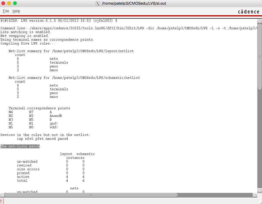
Below are the schematics, symbols, layouts, extracted and DRC/LVS of INVERTER (creates last lab), NAND and XOR gates.
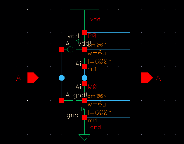
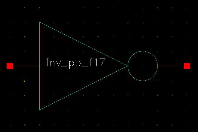
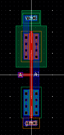
Inverter:
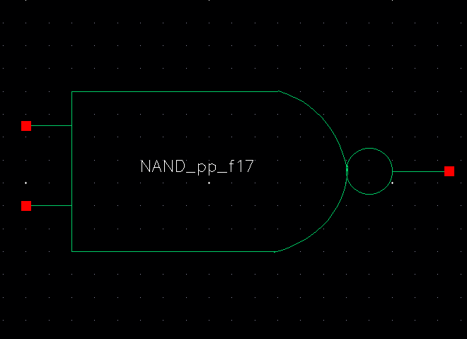
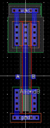
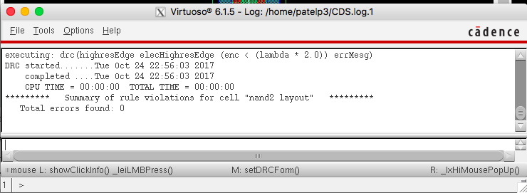
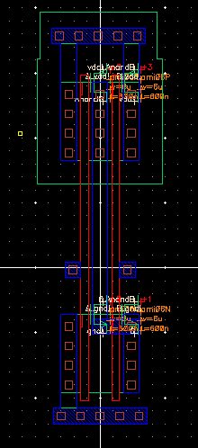
Nand gate:

XOR:
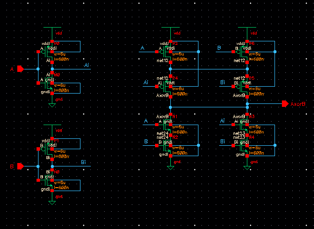

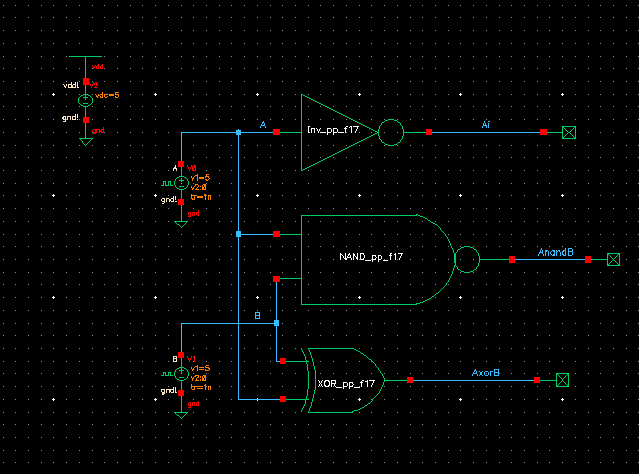
Logic gates:
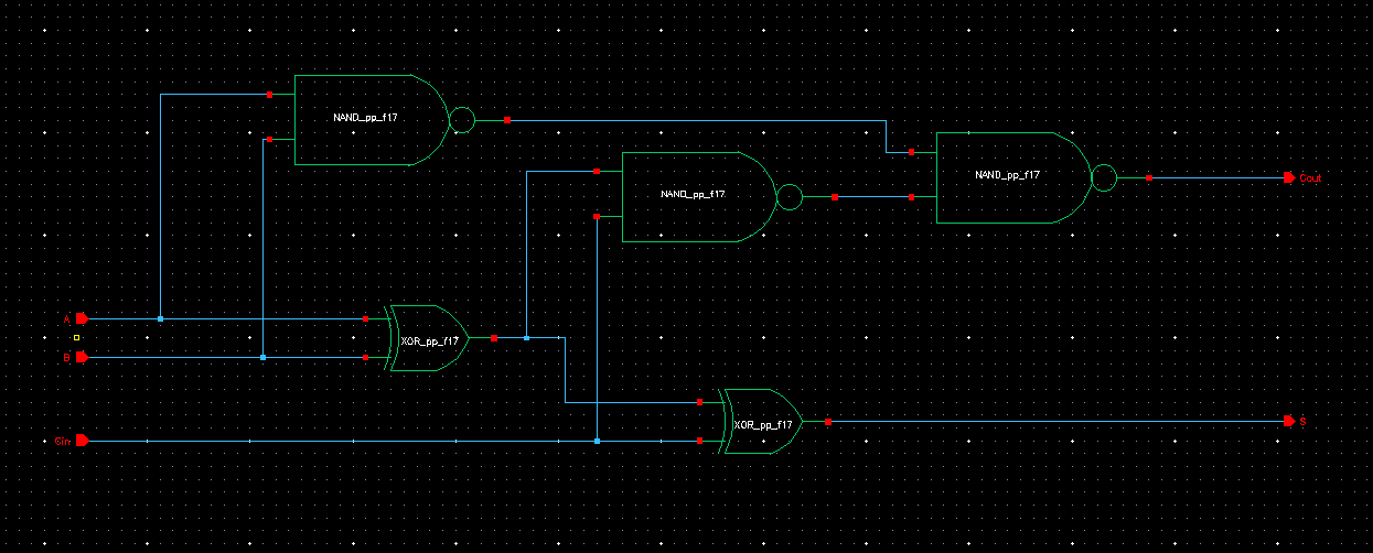
Ths schematic below is a circuit that will follow the binary truth table below:
A
|
B
|
Cin
|
AnandB
|
AxorB
|
0
|
0
|
1
|
1
|
0
|
0
|
1
|
1
|
1
|
1
|
1
|
0
|
0
|
1
|
1
|
1
|
1
|
0
|
0
|
0
|
The logic gates are all connected and VDD is used to power the NMOS and
PMOS gates. The inputs are binary numbers 00,01,10, 11 with different
combinations of two inputs.
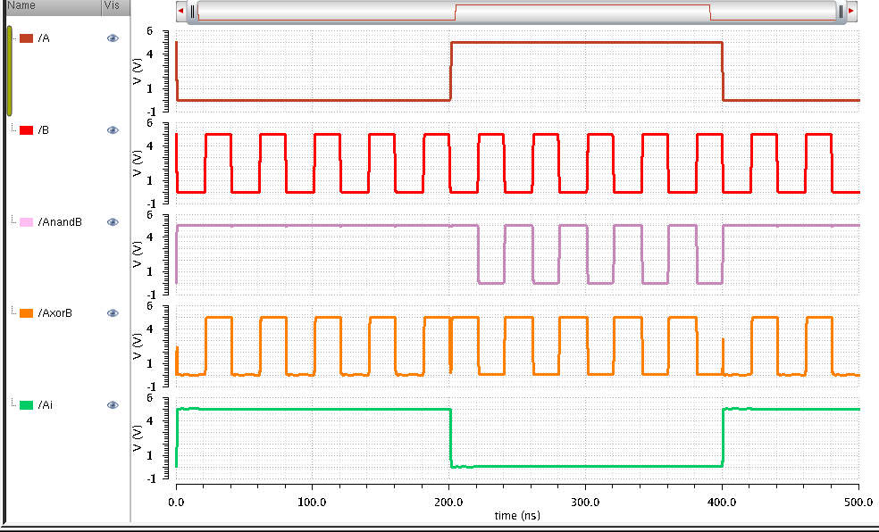
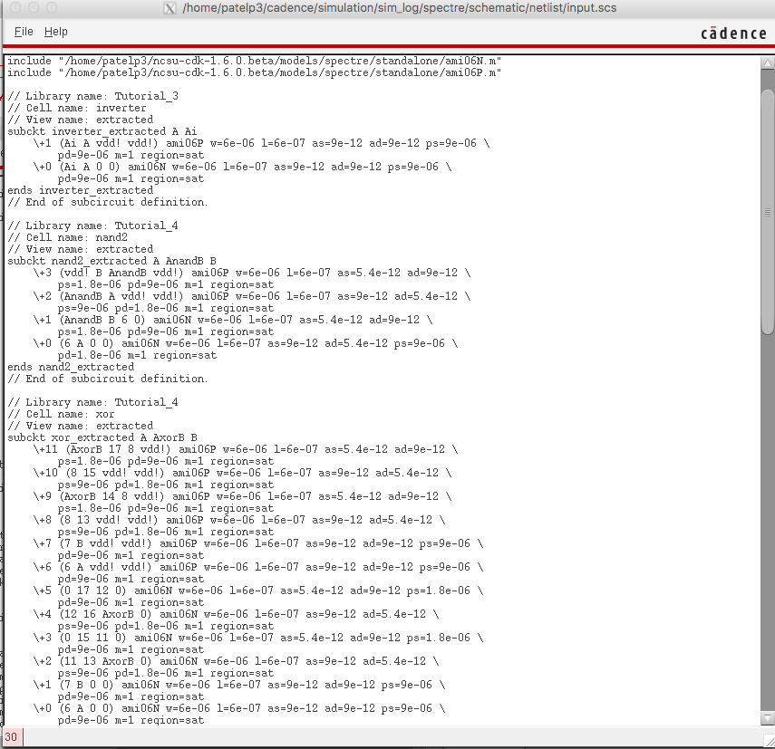
The extracted simulation:

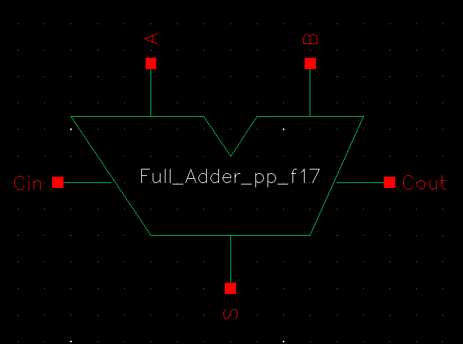
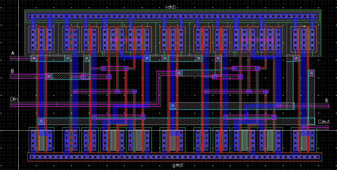
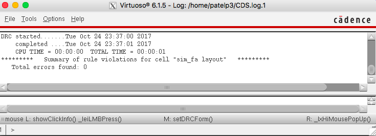
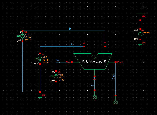
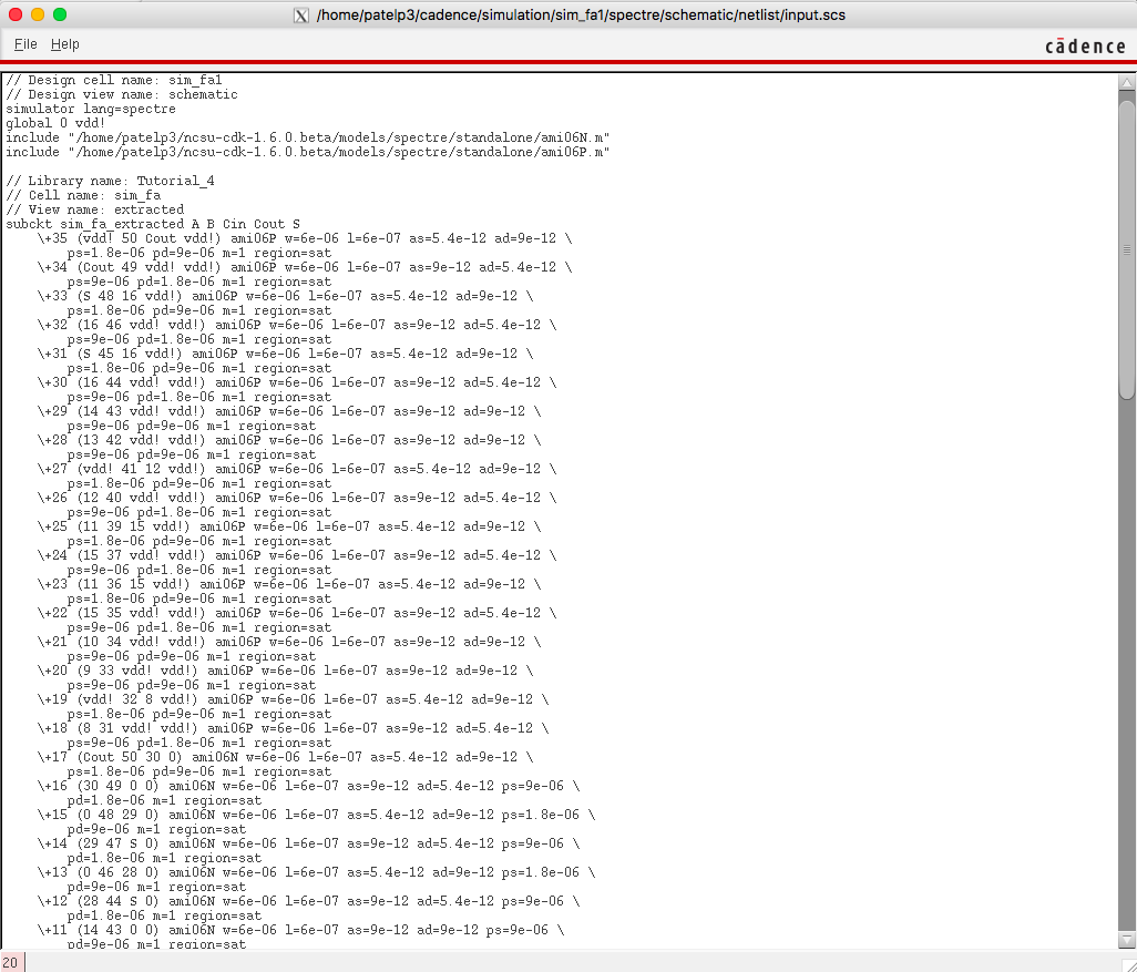
Full Adder:
The full adder is created using the example provided in the lab
instructions. Below is the schematic, symbol, layout, extracted, DRC
and LVS. This Full Adder has three binary inputs (A, B, Cin) and two
outputs (S, Cout). It takes each input individually as a 1-bit input
and uses addition operation.
Full Adder Simulation:
Finally, I added voltage sources to each input that pulsed 0 to 5 at
different delay times to create a random pattern so we can see the
resulting operation of Full Adder. Since there are three inputs, there
are eight different combinations of binary numbers, resulting in
numbers 0 to 7.
A
|
B
|
Cin
|
S
|
Cout
|
0
|
0
|
0
|
0
|
0
|
0
|
0
|
1
|
1
|
0
|
0
|
1
|
0
|
1
|
0
|
0
|
1
|
1
|
0
|
1
|
1
|
0
|
0
|
1
|
0
|
1
|
0
|
1
|
0
|
1
|
1
|
1
|
0
|
0
|
1
|
1
|
1
|
1
|
1
|
1
|
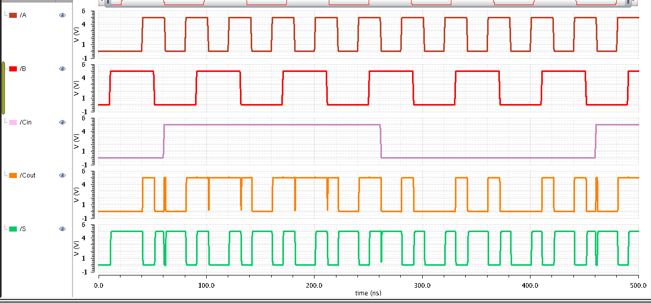
The extracted simulation.

End of Lab 6
Return to labs