Lab 5 - EE 421L
Prachi Patel
patelp3@unlv.nevada.edu
Oct 11, 2017
Pre-lab:
For the prelab we completed Tutorial 3 to create inverter using NMOS
and PMOS. The 12u/6u inverter created was used for Lab 5. Pictures
included in the lab.
Below is my backup work on Google Drive
Lab:
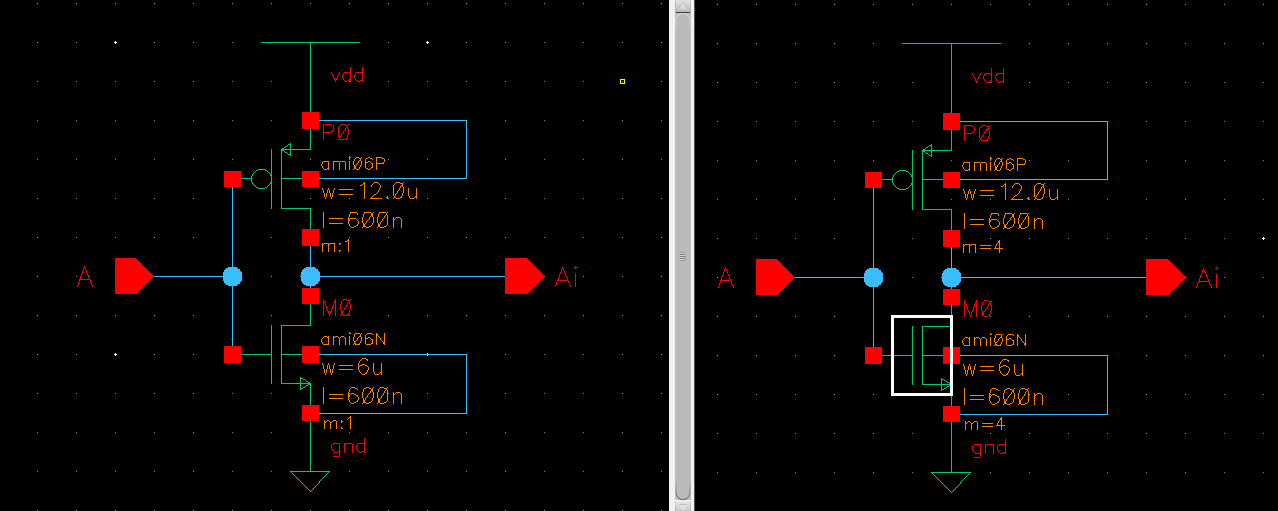
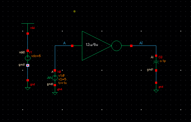
Below
are the schematics for the inverters created using PMOS and NMOS
devices. The 12u/6u inverter was created during the prelab and I used
that to create the 48u/24u by changing the multiplier to m=4.
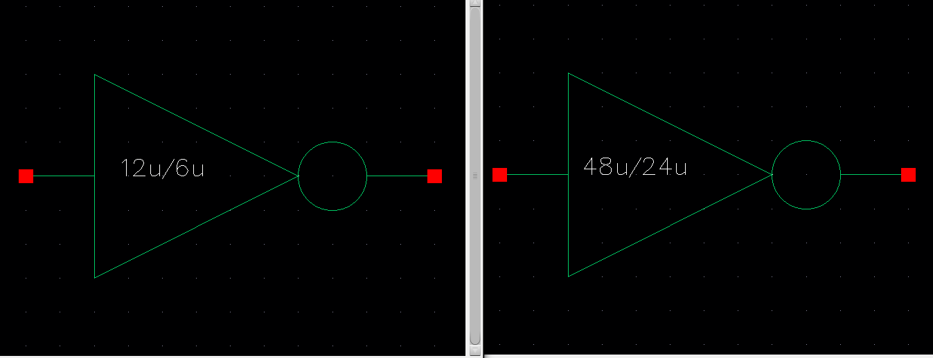
Similarly, the first symbol was created during the prelab and I
created the second symbol for the lab using the 48u/24u schematic.
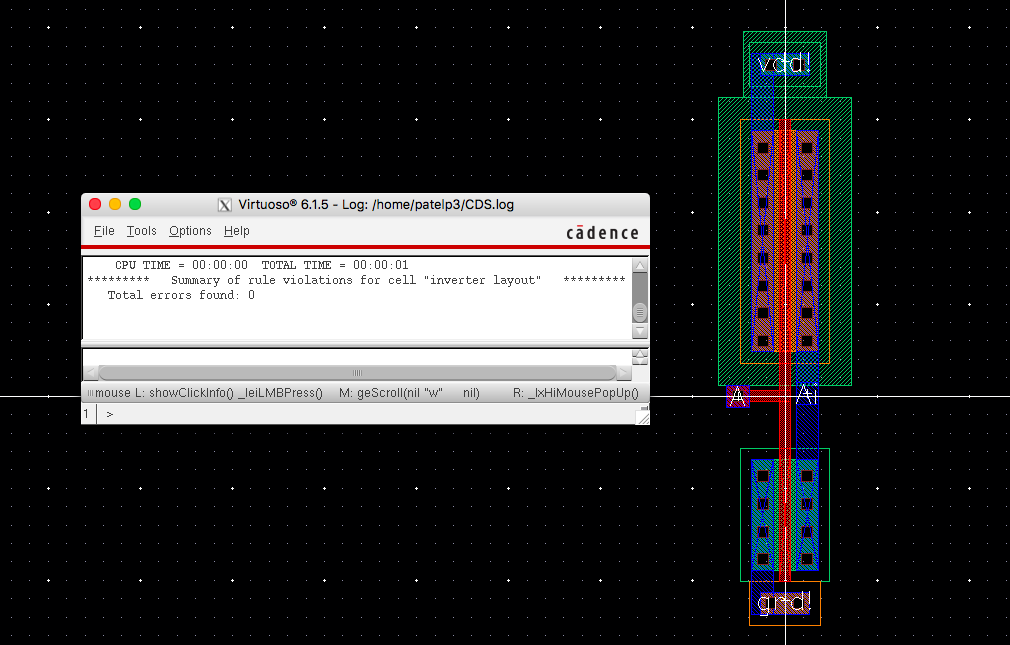
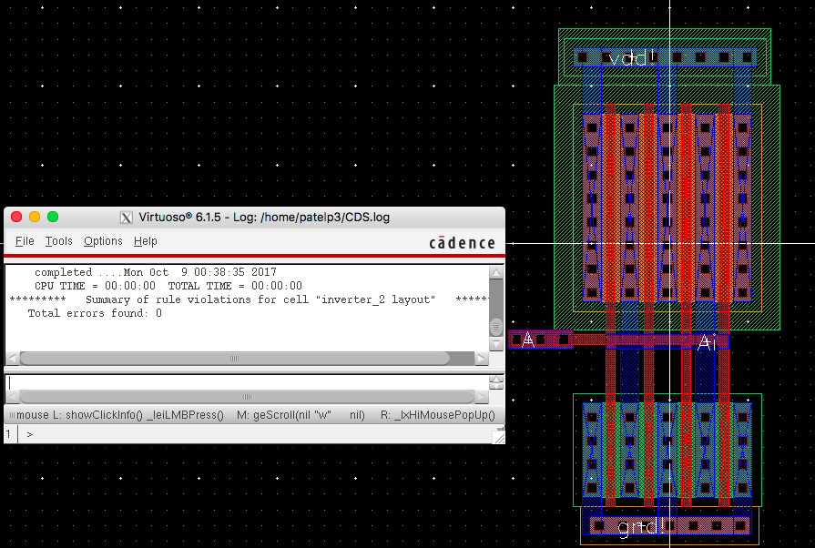
Next was layout for the inverters. First one is for 12u/6u and uses
ntap, pmos, m1_poly, nmos and ptap. For the second one, I changed the
multiplier of 4 again while also changing the rows of ntap, ptap and
m1_poly to match the devices. Below are the layout at display depth 10
and DRC with 0 errors.
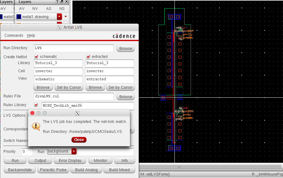
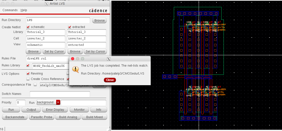
Then I extracted the layouts and ran LVS and as seen below, the netlists matched.
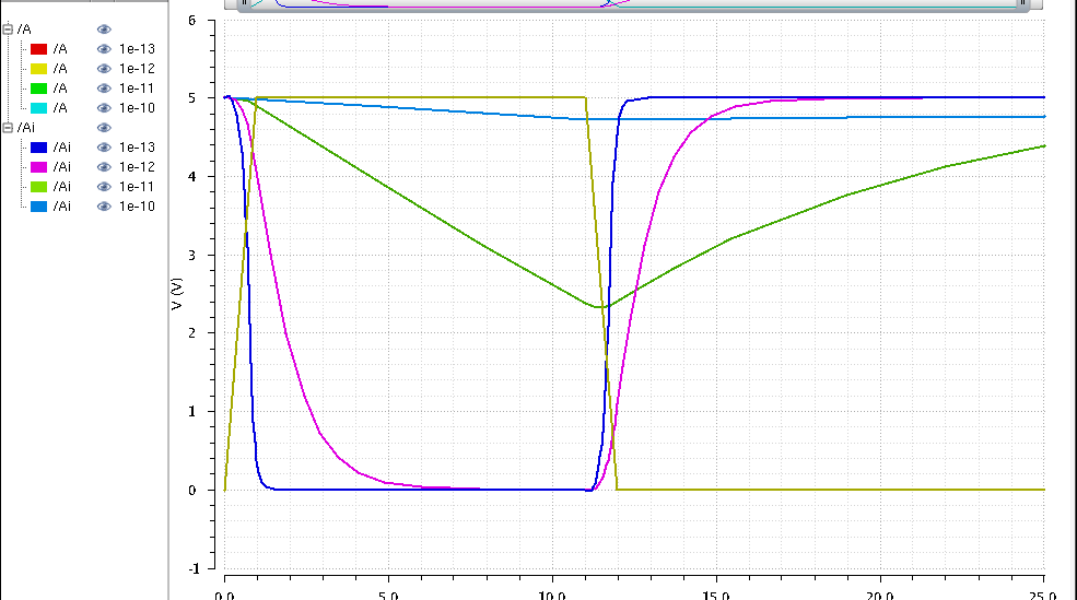
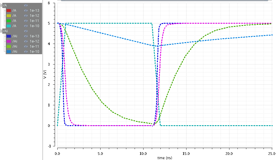
SPICE SIMULATIONS
For the simulations, we were required to use 4 capacitive loads: 100fF,
1fF, 10pF, and 100pF. I attempted two different ways. First, I tested
out by running simulations using each one of them one at a time
directly. Then I used parametric analysis to run them faster and also
made sure the simulations match with the individual ones.
For the analysis, I set the transient analysis to 25ns in Ultrasim and
used A and Ai for the output plots. In the parametric analysis, I set
the value of C to 0 and then ran the range from 100f to 100p on auto
step mode with 4 steps.
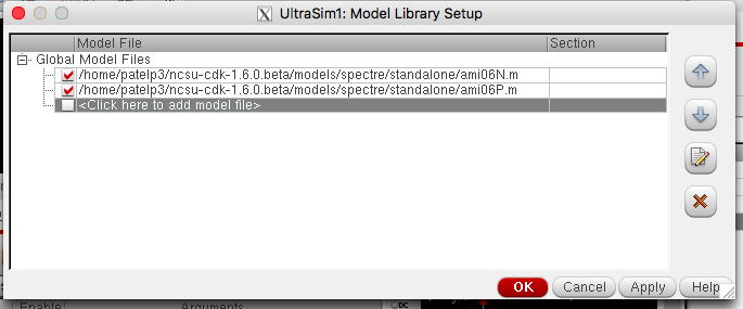
The model libraries used for pmos and nmos devices simulations.
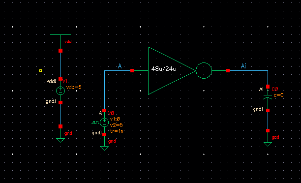
Here are the results. First simulation for 12u/6u and second simulation is for 48u/24u.
The cadence files for the lab 5 can be downloaded here: lab5_pp.zip
End
Return to the labs