Lab 3 - EE 421L
Prachi Patel
patelp3@unlv.nevada.edu
Sept 27, 2017
Pre-lab:
For the prelab we completed Tutorial 2 and used the NMOS and PMOS created for the lab.
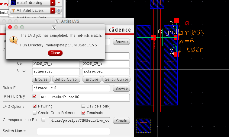
This is NMOS LVS.
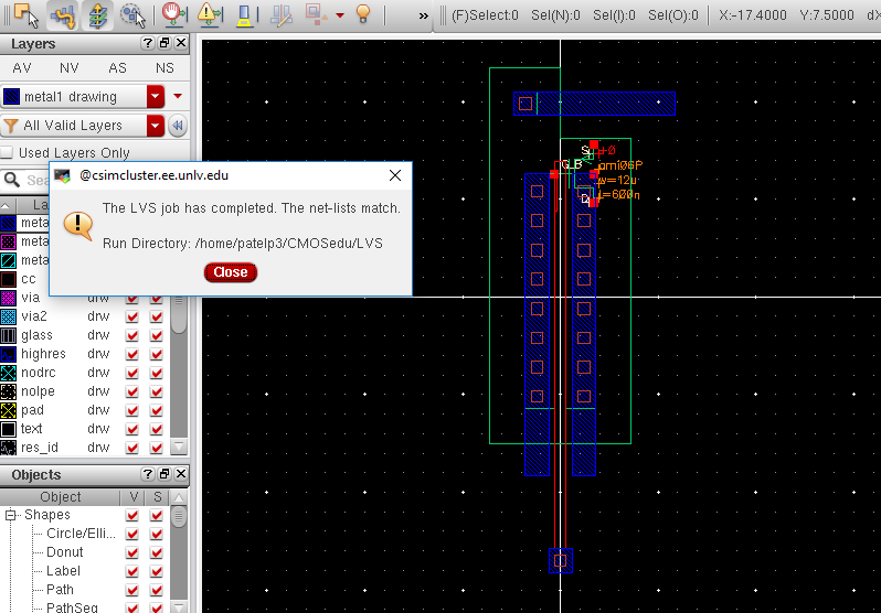
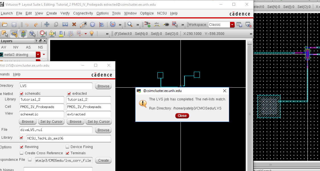
This is PMOS LVS
Drive updated below.
LAB 4:
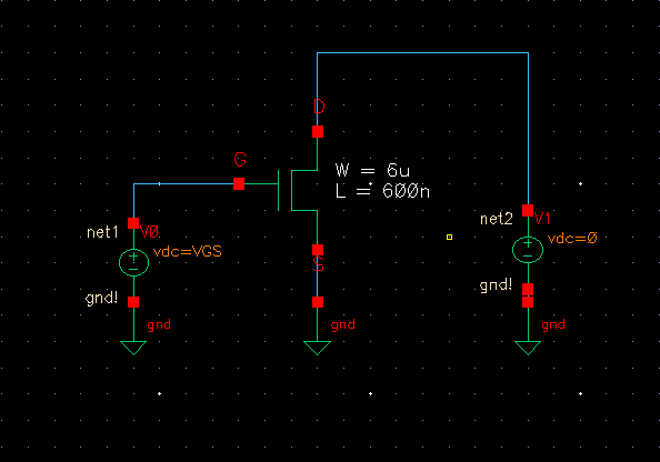
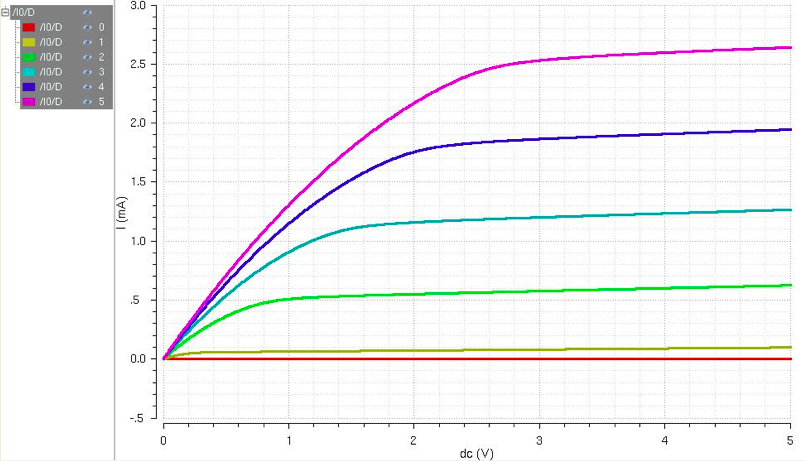
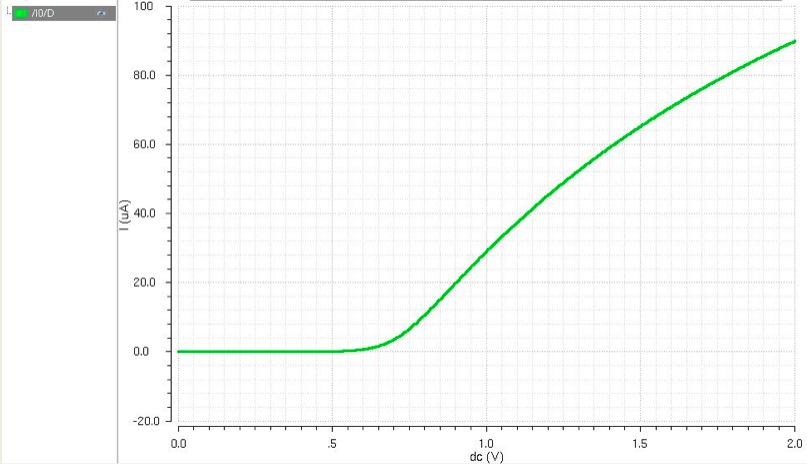
NMOS
ID vs VDS and ID vs VGS for NMOS device
1. VGS varies 0 to 5 in 1V steps, VDS varies 0 to 5 in 1mV steps
2. VGS varies 0 to 2 in 1mV steps, VDS is 100mV
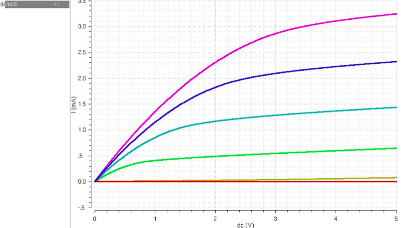
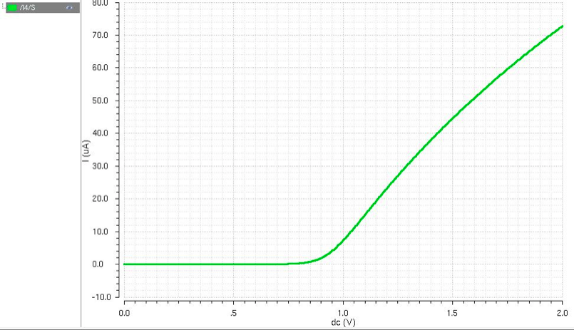
PMOS
ID vs VSD and ID vs VSG for PMOS device
1. VSG varies 0 to 5 in 1V steps, VSD varies 0 to 5 in 1mV steps
2. VSG varies 0 to 2 in 1mV steps, VSD is 100mV
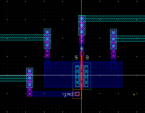
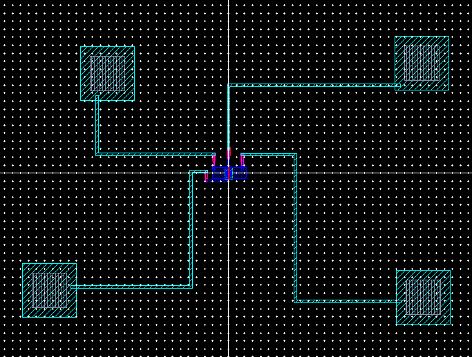
NMOS - Probepads
I
used two different kinds of methods to connect the NMOS and PMOS we
created in prelab to the probepads. For the NMOS, I used m2_m1 and
m3_m1 to connect the three different methdos. However, that gave me a
lot of errors and though I was able to DRC is after a lot of struggle,
I found the second method easier.
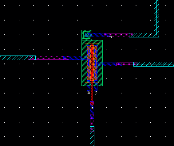
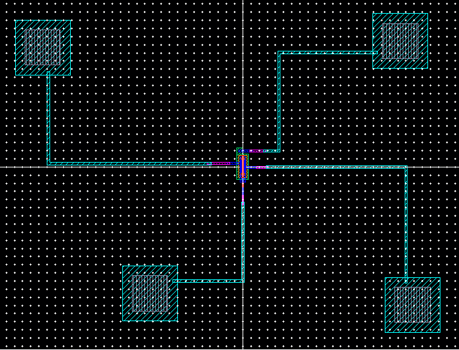
PMOS - Probepads
For this one, I went straight into the easier method and avoided the
m2_m1 and m3_m2 layouts. I connected metal1 to metal2 directly and
metal2 to metal3 similarly, making sure to keep the width of the wires
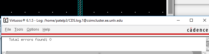
matching. DRC and LVS to the scehmatic provided in the lab4 zip is
below.
Lab4 items in Tutorial2_zip
Return to the labs