Lab 3 - EE 421L
Prachi Patel
patelp3@unlv.nevada.edu
Sept 20, 2017
Pre-lab:
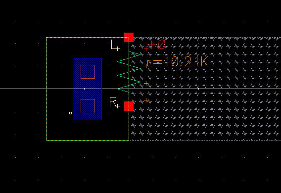
For this prelab, I completed this the rest of the Tutorial 1. I created
a simple circuit with 10k resistors and converted that into a symbol.
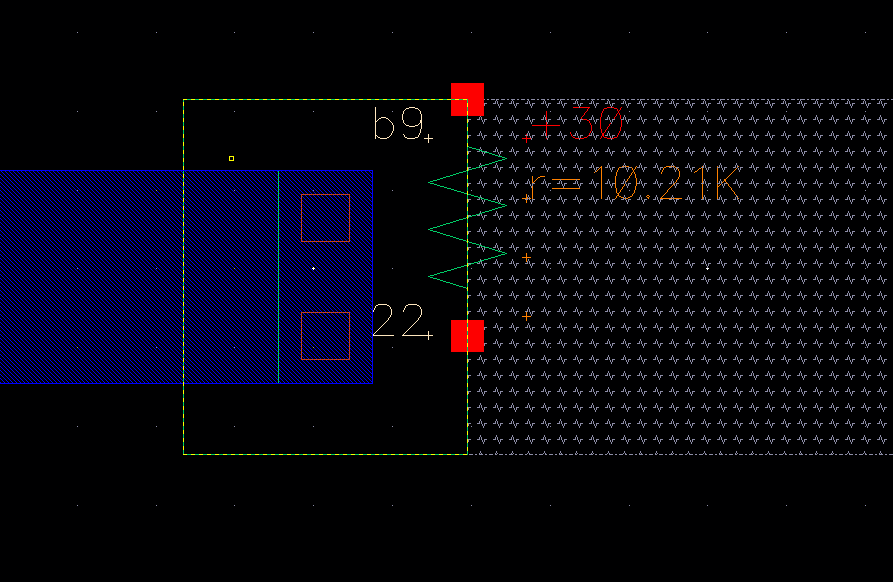
Then using n-well in layout, I created approx 10k resistor which
turned out to be 10.21k when I extracted the design. Next, I
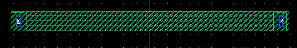
tried to recreate the circuit that we had initially created. After
connecting the resistors with the metal, I did an LVS that stands for
layout vs schematic. I had to be play around a bit with the pin
dimension, input, output and terminal names until the netlist matched.
LAB
To calculate the width and length of N-Well resistor, we use the
equation R = ρ*(L/W) where R is the total resistance, ρ is the sheet
resistance (Ohms/Square), L is the length and W is the width. Taking
the sheet resistance to be about 800, we find L and W that will satisfy
the 10K resistor. W must be at least 3.6 um. If we use 3.6 as our W,
then L must be 45um. I created a 10K N-Well resistor for prelab and
used it to create DAC Layout.
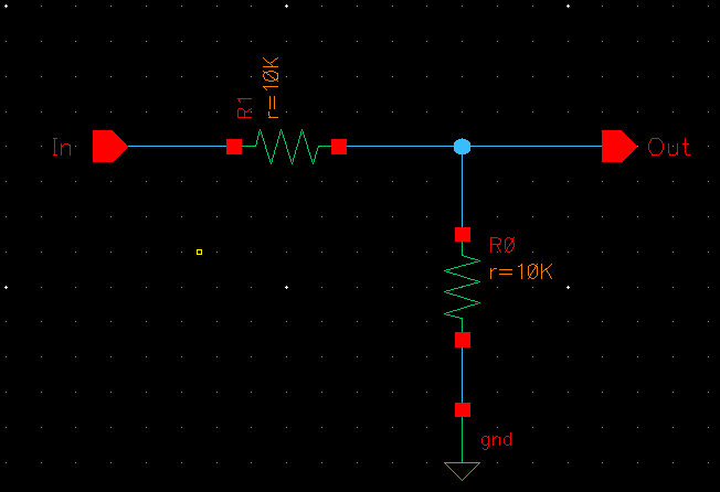
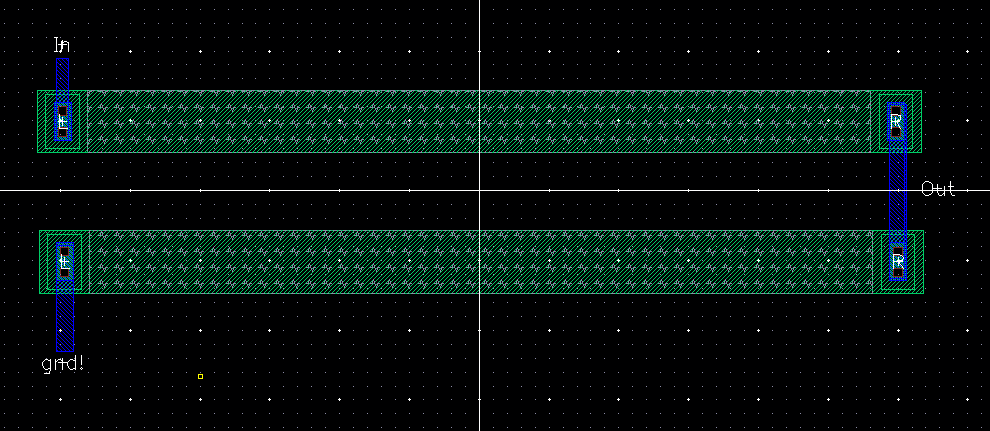
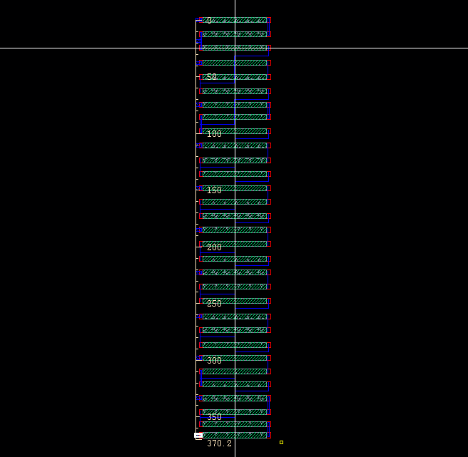
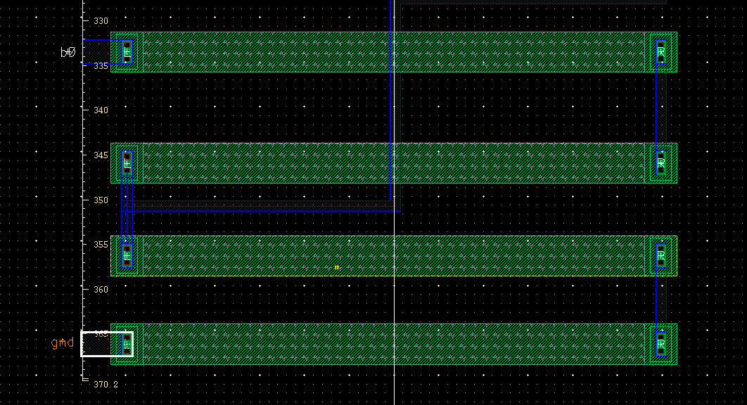
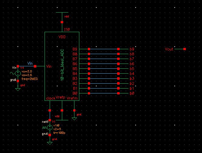
We created a DAC schematic last lab and using that schematic, I created
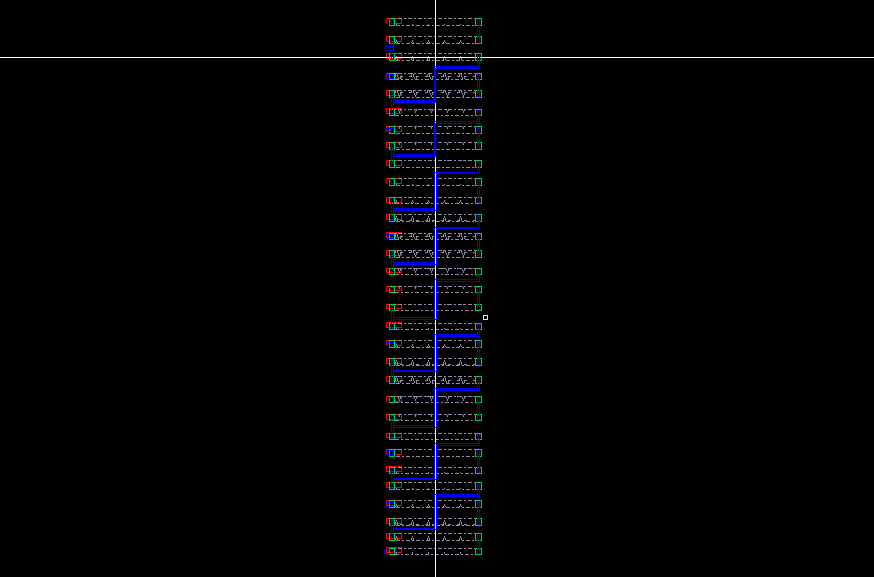
a layout with two 10K resistors in series and one in parallel. The DAC
is a 10-bit so there are total 10 such set of 3 resistors. The
connections were done using metal 1 over L & R pins that were
already there form prelab.

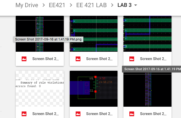
As seen above, DRC passed so I went ahead and extracted the layout. The
resistor was 10.2K which was within error margin so the layout was okay
to proceed with.
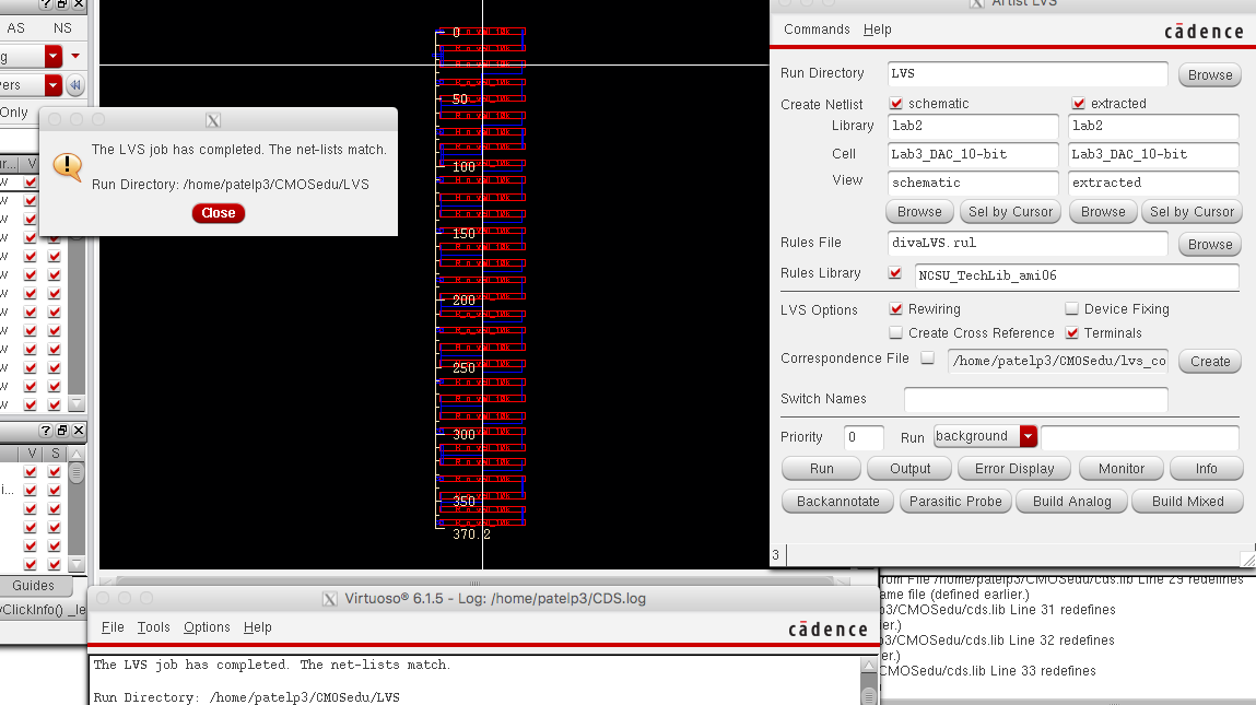
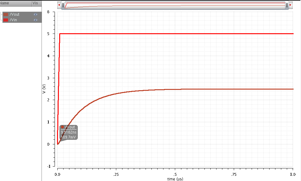
I ran LVS to do a Layout vs. Schematic which passed, as seen above.
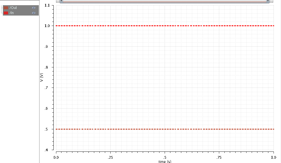
Then to check the simulations, I used the edited symbol and ran it
using the schematic from Lab 2.
Download the Cadence zip folder here - Lab3.zip
Return to the labs