EE 421L
Lab 7
Authored
by Jeremy Morgan
Email: morgaj7@unlv.nevada.edu
Due: 11/8/2017
Pre-lab:
Back-up all of your work from the lab and the course.
Go Through Tutorial 5
Lab:
Part 1: 4-bit Inverter Analysis)
4-bit Inverter:
Symbol

Schematic
1bit
Schematic 8bit


Simulation + Results


The capacitatative load connected to the outputs effected the signals greatly.
We see as the capacitance increases, rise and fall time also increase in the output.
Part 2: Create schematics and symbols for an 8-bit input/output array of: NAND, NOR, AND, inverter, and OR gates.)
Or:
Symbol

Schematic
1bit
Schematic 8bit


Simulation + Results


Nor:
Symbol

Schematic
1bit
Schematic 8bit


Simulation + Results


Nand:
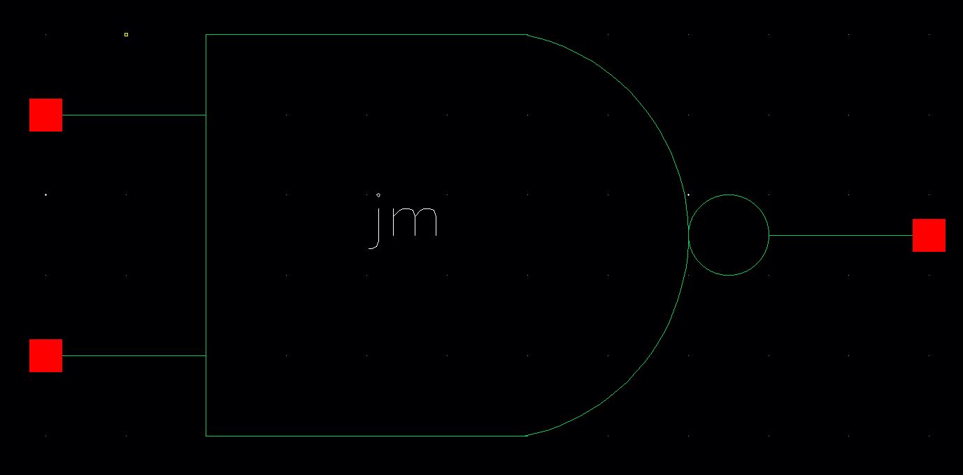
Symbol

Schematic
1bit
Schematic 8bit


Simulation + Results


And:
Symbol

Schematic
1bit
Schematic 8bit


Simulation + Results


Inverter:
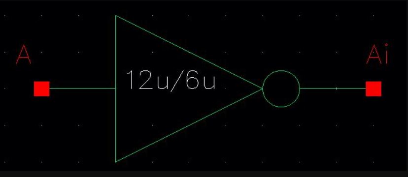
Symbol

Schematic
1bit
Schematic 8bit


Simulation + Results


Part 3: 2-to-1 Demux/Mux analysis:
2 - to -1 Mux has a single select line.
There are two inputs (in this case A and B) and an output (Z) that is dependent on 'S'
2 - to - 1 MUX:
Symbol
Schematic 1bit


Simulation + Results


2 - to - 1 MUX (With Inverter):
Symbol
Schematic 1bit


Simulation + Results


8 BIT : 2 - to - 1 MUX:
Symbol
Schematic 8bit


Simulation + Results


HOW IT WORKS:
8-Bit Mux:
When S is equal to 1, Z goes to A.
When S is equal to 0, Z goes to B.
8 bit 2- to - 1 DEMUX:
Symbol
Schematic 8bit


Simulation + Results


HOW IT WORKS:
8-Bit DEMux:
When S is equal to 1, Z goes to A.
When S is equal to 0, Z goes to B.
Part 4: 8-bit Full Adder Analysis)
8 bit Full Adder:
Symbol

Schematic
1bit
Schematic 8bit


Simulation + Results


S7, S6, S5, S4, S3, S2, S1, S0 all depict the same data.
Return to EE 421L Labs