EE 421L
Lab 6
Authored
by Jeremy Morgan
Email: morgaj7@unlv.nevada.edu
Due: 10/25/2017
Pre-lab:
Back-up all of your work from the lab and the course.
Go Through Tutorial 4
Lab:
Part 1: Draft the schematics/layout/symbol of a 2-input NAND and XOR gate
6u/600n NAND:
Schematic:
Symbol View:


For the Layout and Extracted view, only used 1 row of contacts on VDD and Ground to reduce layout size.
A larger than neccessary standard cell height was used for future additions
Layout requires 4 pins : A - B - Gnd - VDD
The schematic only needs two pins: A - B
Layout View:
Extracted View:


DRC the 6u/600n NAND layout:

LVS of the 6u/600n NAND Schematic with the Extracted Layout to see if they match:

The Netlists Match
6u/600n XOR:
Schematic:
Symbol View:

For the Layout and Extracted view, only used 1 row of contacts on VDD and Ground to reduce layout size.
A larger than neccessary standard cell height was used for future additions
Layout requires 4 pins : A - B - Gnd - VDD
The schematic only needs two pins: A - B
Layout View:
Extracted View:


DRC the 6u/600n XOR layout:
LVS of the 6u/600n XOR Schematic with the Extracted Layout to see if they match:

The Netlists Match
Part 2: Using Spectre simulate the logical operation of the gates for all 4 possible inputs (00, 01, 10, and 11)
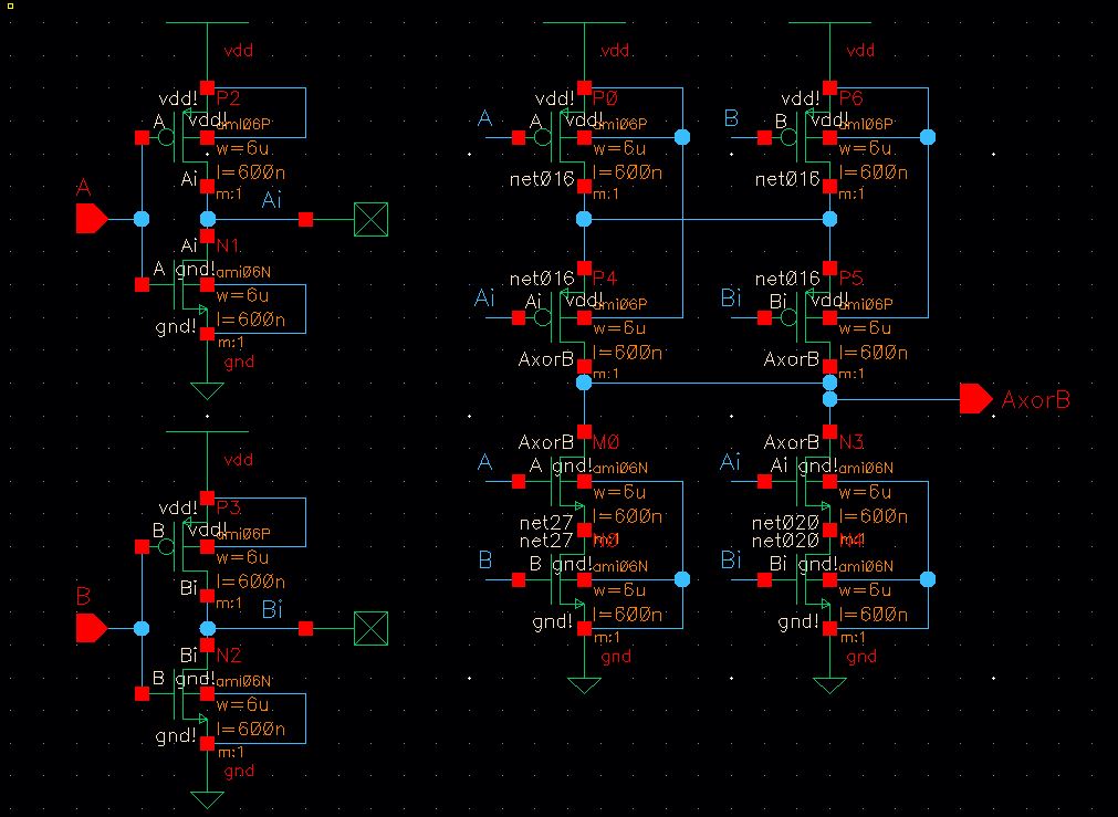
Logic Gate
Schematic:
SPICE: Logical Operator of Gates for all 4 possible inputs


From the graph one will notice glitches.
Timing of the input pulses can cause glitches in the output of the gates.
Due to the nature of capacitance, stored charge causes misfires for the output of the gates.
Gates are read as being both ON and OFF as they are falling at the same time as they are rising.
This causes the Output of the AXORB to be glitched at that time as it does not know what to do in that instance.
Part 3: Draft the schematics/layout/symbol of a FULL ADDER
FULL ADDER:
Schematic:
Symbol View:


For the Layout and Extracted view, utilized previously constructed NAND and XOR and routed using metals 1 and 2.
Layout constructed by placing 5 gates end-to-end so VDD! and GND! are routed
Layout View:
Extracted View:


DRC the FULL ADDER:
LVS of the FULL ADDER using schematic and layout:

The Netlists Match
Part 4: Using Spectre simulate the logical operation of the FULL ADDER
FULL ADDER
Schematic:
SPICE: Logical Operator of Gates for all 4 possible inputes


The same glitch as the XOR can be seen for the summation operation
The Logical Operations depicted in the SPICE MODEL coincide with the logic table for a FULL ADDER:

Lab 6 Files: HERE
Return to EE 421L Labs