EE 421L
Lab 5
Authored
by Jeremy Morgan
Email: morgaj7@unlv.nevada.edu
Due: 10/11/2017
Pre-lab:
Back-up all of your work from the lab and the course.
Go Through Tutorial 3
Lab:
Part 1: Draft schematics, layouts, and symbols for two inverters)
12u/6u Inverter:
(width of the PMOS / width of the NMOS with both devices having minimum lengths of 0.6u)
Schematic:
Symbol View:


For the Layout and Extracted view, only used 1 row of contacts on VDD and Ground to reduce layout size.
Layout requires 4 pins : Ai - A - Gnd - VDD
The schematic only needs two pins: A - Ai
Layout View:
Extracted View:


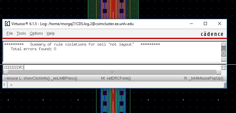
DRC the 12u/6u inverter layout:
LVS of the 12u/6u Inverter Schematic with the Extracted Layout to see if they match:
The Netlists Match
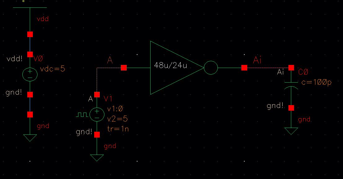
48u/24u Inverter:
(Device uses 4x multiplyer [ m = 4] to achieve 48u/24u inverter)
(m=4 is detailed within the schematic below)
Schematic:
Symbol View:


For the Layout and Extracted view, only used 1 row of contacts on VDD and Ground to reduce layout size.
Layout requires 4 pins : Ai - A - Gnd - VDD
The schematic only needs two pins: A - Ai
Layout View:
Extracted View:


DRC the 48u/24u inverter layout:
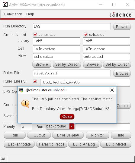
LVS of the 48u/24u Inverter Schematic with the Extracted Layout to see if they match:

The Netlists Match
Part 2: Using SPICE and ULTRASIM simulate the operation of both inverters driving a 100 fF, 1 pF, 10 pF, and 100 pF capacitive load)
12u/6u Inverter:
100fF Capactive Load:
Schematic:
SPICE:


UltraSim:
1pF Capactive Load:
Schematic:
SPICE:


UltraSim:
10pF Capactive Load:
Schematic:
SPICE:


UltraSim:
100pF Capactive Load:
Schematic:
SPICE:


UltraSim:
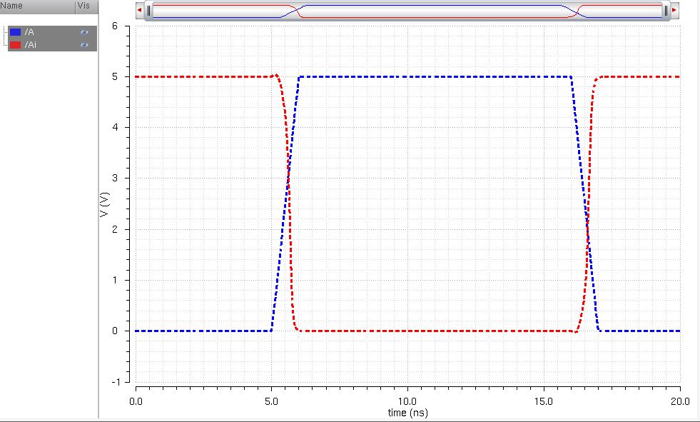
From the above schematics and spice responses one can deduce that the capicitative load has had an effect on the waveform of Ai.
The time delay between A and for Ai to map is increased with the capacitative load.
Due
to this fact the waveforms of Ai also become sharper/steeper as the
capacitance increased because of the output signal being dimished
in quality.
This diminshment in quality is due to the fact that the
capacitors could not reach a fully charged state in the time between
pulses.
48u/24u Inverter:
100fF Capactive Load:
Schematic:
SPICE:

UltraSim:
1pF Capactive Load:
Schematic:
SPICE:


UltraSim:
10pF Capactive Load:
Schematic:
SPICE:


UltraSim:
100pF Capactive Load:
Schematic:
SPICE:

UltraSim:
The above schematic and graphing for the 48u/24u inverter show the same trend as the 12u/6u inverter's results.
Once again it can be seen that the time delay between A and for Ai to map is increased with the capacitative load.
And as previously stated, due to this fact, the waveforms of Ai also become sharper/steeper as the
capacitance increased because of the output signal being dimished in
quality.
However
with the 48u/24u inverter being used, the diminishing of quality and
time delay were less exagerated then the 12u/6u counterpart up to a
certain point.
Lab 5 Files: HERE
Return to EE 421L Labs