EE 421L
Lab 4
Authored
by Jeremy Morgan
Email: morgaj7@unlv.nevada.edu
Due: 9/27/2017
Pre-lab:
Back-up all of your work from the lab and the course.
Go Through Tutorial 2
Lab:
Part 1: Generating 4 Schematics with Simulations for NMOS and PMOS Analysis)
1.
- A schematic for simulating ID
v. VDS of an NMOS device for VGS varying from 0 to 5 V in 1 V steps
while VDS varies from 0 to 5 V in 1 mV steps. Using a 6u/600n
width-to-length ratio.


To Simulate this Layout, Used a linear step size while also using a parametric analysis. That gives us the 6 values.
Linear Step ADL :
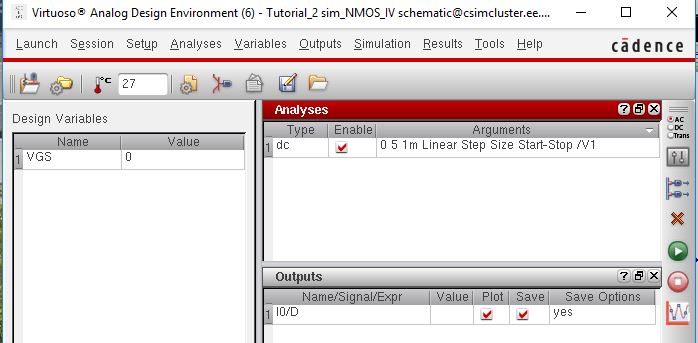
Parametric Analysis:

2.
- A
schematic for simulating ID v. VGS of an NMOS device for VDS = 100 mV
where VGS varies from 0 to 2 V in 1 mV steps. Using a 6u/600n
width-to-length ratio.


Analog Design Environment:

3.
- A
schematic for simulating ID v. VSD (note VSD not VDS) of a PMOS device
for VSG (not VGS) varying from 0 to 5 V in 1 V steps while VSD varies
from 0 to 5 V in 1 mV steps. Use a 12u/600n width-to-length ratio.


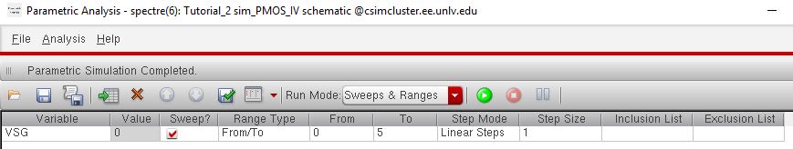
To Simulate this Layout, Used a linear step size while also using a parametric analysis. That gives us the 6 values.
Linear Step ADL :

Parametric Analysis:
4.
- A
schematic for simulating ID v. VSG of a PMOS device for VSD = 100 mV
where VSG varies from 0 to 2 V in 1 mV steps. Again, use a 12u/600n
width-to-length ratio.

Analog Design Environment:

Part 2: Lay out a 6u/0.6u NMOS and PMOS device and connect all 4 MOSFET terminals to probe pads)
Lay out a 6u/0.6u NMOS device and connect all 4 MOSFET terminals to probe pads.
NMOS Device:

Connecting to Probe Pads:
Full
Layout View:
Extracted Layout View:


Layout Passing DRC:


Schematic to be Compared with Layout Using LVS:

LVS Between Schematic and Layout: LVS shows both match

Lay out a 6u/0.6u PMOS device and connect all 4 MOSFET terminals to probe pads
PMOS Device:

Connecting to Probe Pads:
Full
Layout View:
Extracted Layout View:


Layout Passing DRC:
Schematic to be Compared with Layout Using LVS:

LVS Between Schematic and Layout: LVS shows both match

Lab 4 Files: HERE
Return to EE 421L Labs
