EE 421L
Lab 2
Authored
by Jeremy Morgan
Email: morgaj7@unlv.nevada.edu
Due: 9/13/2017
Lab
description:
In
this lab we'll use n-well resistors to implement a 10-bit DAC. We will
verify this with an ideal DAC and utilize our 10 bit DAC for different
loads.
Prelab:
1. Defining Proper Libraries
Unzipped Lab2 directory file into Cmosedu/Cadence.
Defined correct libraries using Cds.lib with DEFINE command.
2. Simulating Ideal_ADC_DAC
Opened newly added Ideal ADC DAC simulation using cadence:

Simulated Input vs Output of above schematic

The output voltage is limited to 5v as that is the VDD of the 10 bit DAC System.
This phenomonen is illustrated by making Vin much larger but Vout is still only 5 volts at its peak.
It flatlines at 5 volts.

THE
LSB of the DAC is said to be the LEAST SIGNIFICANT BIT, or, in other
words, the lowest amount of voltage that can go through a single
bit.
The Formula for the LSB is: VDD / 2^(n*10).
n = number of bits within system, 10 bits in our case.
VDD = voltage going into DAC, 5v in our case.
LSB for this system is 5v / 2^(10*10).
LSB = 4.88 mV.
This will only hold true if the 5v VDD is to be confirmed which with the above graph, it has been.
Lab Work
1. The design of a 10-bit DAC using an n-well R of 10k and Symbol View)
Construction of 10 bit DAC:

Construct symbol view of 10 Bit Dac above.
(Create -> Cellview -> new Cell View)

Determine the Output Resistance of the system:
For each bit the resistor in parrallel in series engage in a repetive sequence in which each output is 1R

Starting from the intial point above in which the resistance is equal to 2R // 2R which is just R.
The sequence continues down each bit until we reach the end where the Reistance is seen just to be R.
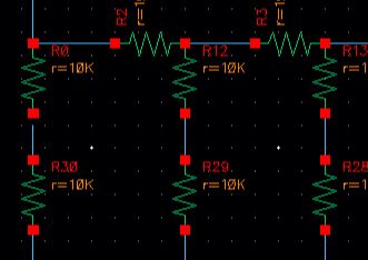
Thus the total Resistance is just R = 10k
2. Delay when Driving a Capacitative Load).

Because of the nature of the system above, the voltage going out of the system should be delayed.
This delay can be represented by the time delay formula: .7 * Resistitance * Capacitance.
R = 10k C = 10pF
Time Delay should be equal to 10k * 10pF * .7 giving 70ns
The solution is verified as 74.86 ns - 5ns (intrinsic) will equal 69.86 ns

3. Verification of Symbol Design)
To verify the design of my chip, I will be comparing my new simulations to the original 'Ideal' Schematic:
Ideal Schematic:

Schematic with my 10 bit DAC:


The Ideal graph and the graph in which the constructed 10 bit DAC was used show an almost identical graph for Vin and Vout.
The constructed 10 bit DAC is working and verified.
4. Driving Loads)
Resistive Load:


What happens if the DAC drives a 10k load?
When constructing a 10k resistive load with the DAC, Vout becomes half of Vin.
This is caused by a voltage divider circuit being created when the original 10k becomes in parallel with another 10k load.
Capacitive Load:


Load with Resistor and Capacitor:


What happens if the DAC drives a 10k load?
(explained in Resistive Load schematic)
What happens if the resistance of the switches isn't small compared to R?
The output voltage will lower as the resistance of the switches will add to the overall resistance of the system.
Return to EE 421L Labs