Lab Project - EE 421L
Lab Report:
Inverter:
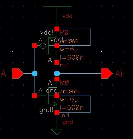
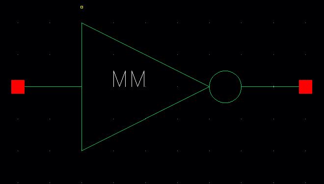
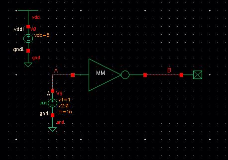
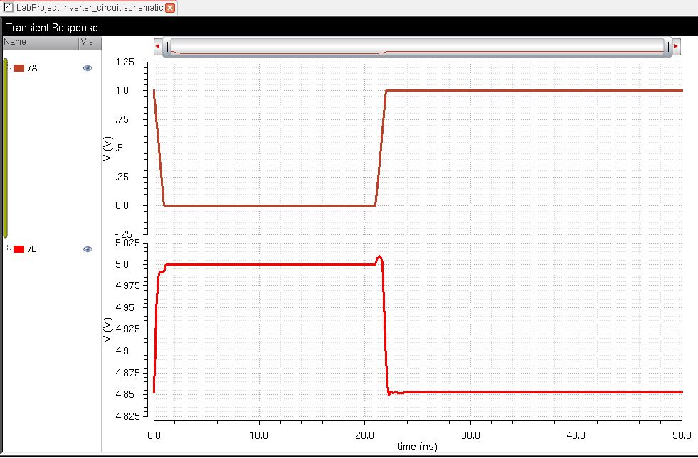
In order to create a parity checking circuit with XOR gates, an inverter needed to be created so it can be added to the circuit. I acquired this inverter from one of my previous labs and simulated it to make sure it worked. With an input of 0, I recieved an output of 1.
| Schematic | Symbol | Simulation Schematic | Simulation |
| | | |
| Layout | Extracted |
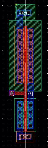 |  |
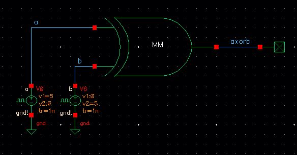
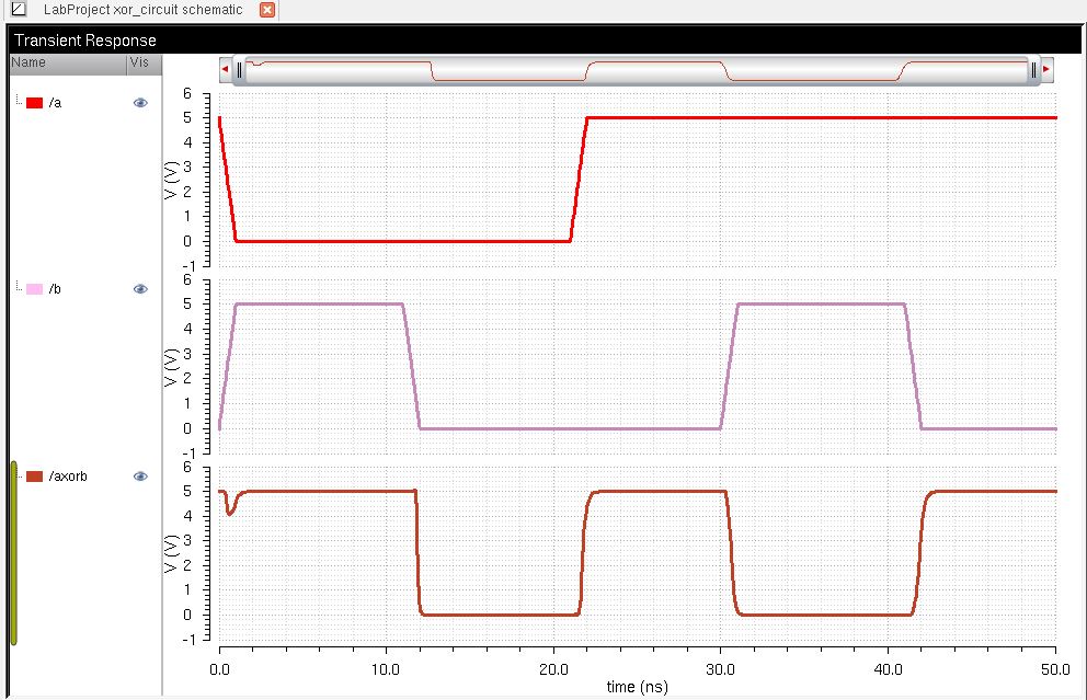
Xor Gate:
The XOR gate used in this project was also acquired from a previous lab I did and to make sure it worked I made a simulation schematic out of it and simulated it. With two inputs (A=0,B=1) the output was a 1.
| Schematic | Symbol | Simulaiton Schematic | Simulation |
 |  |  |  |
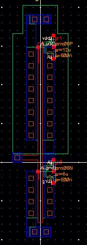
| Layout | Extracted |
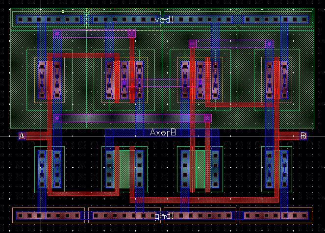 | 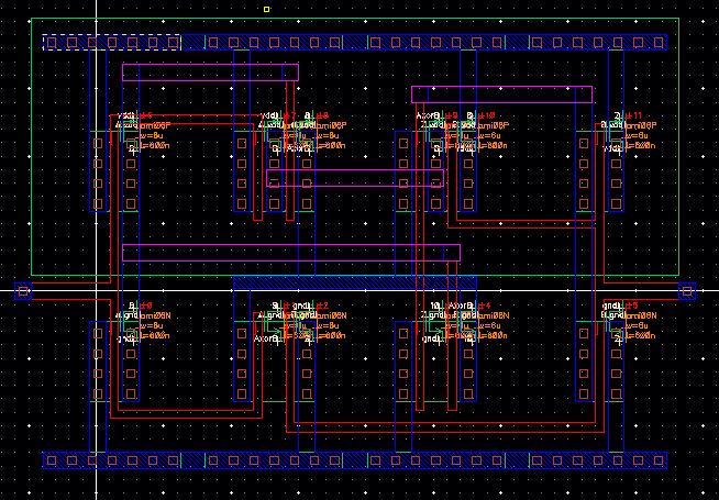 |
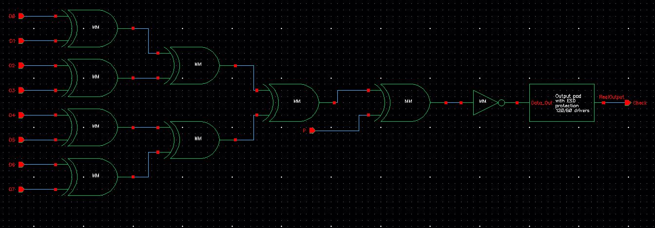
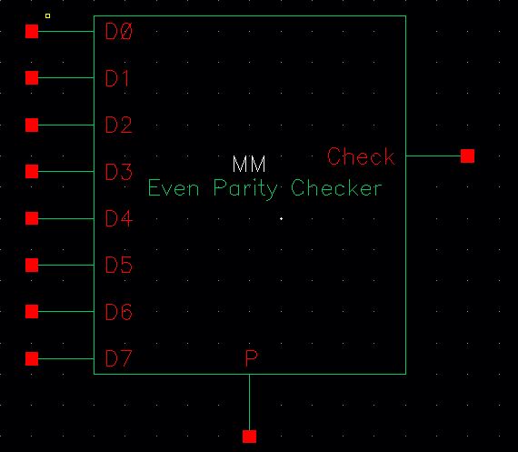
Even Parity Checker:
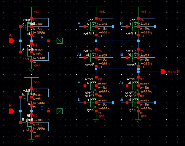
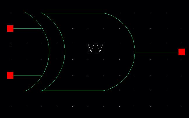
| Schematic | Symbol |
 |  |
| Layout | Extracted |
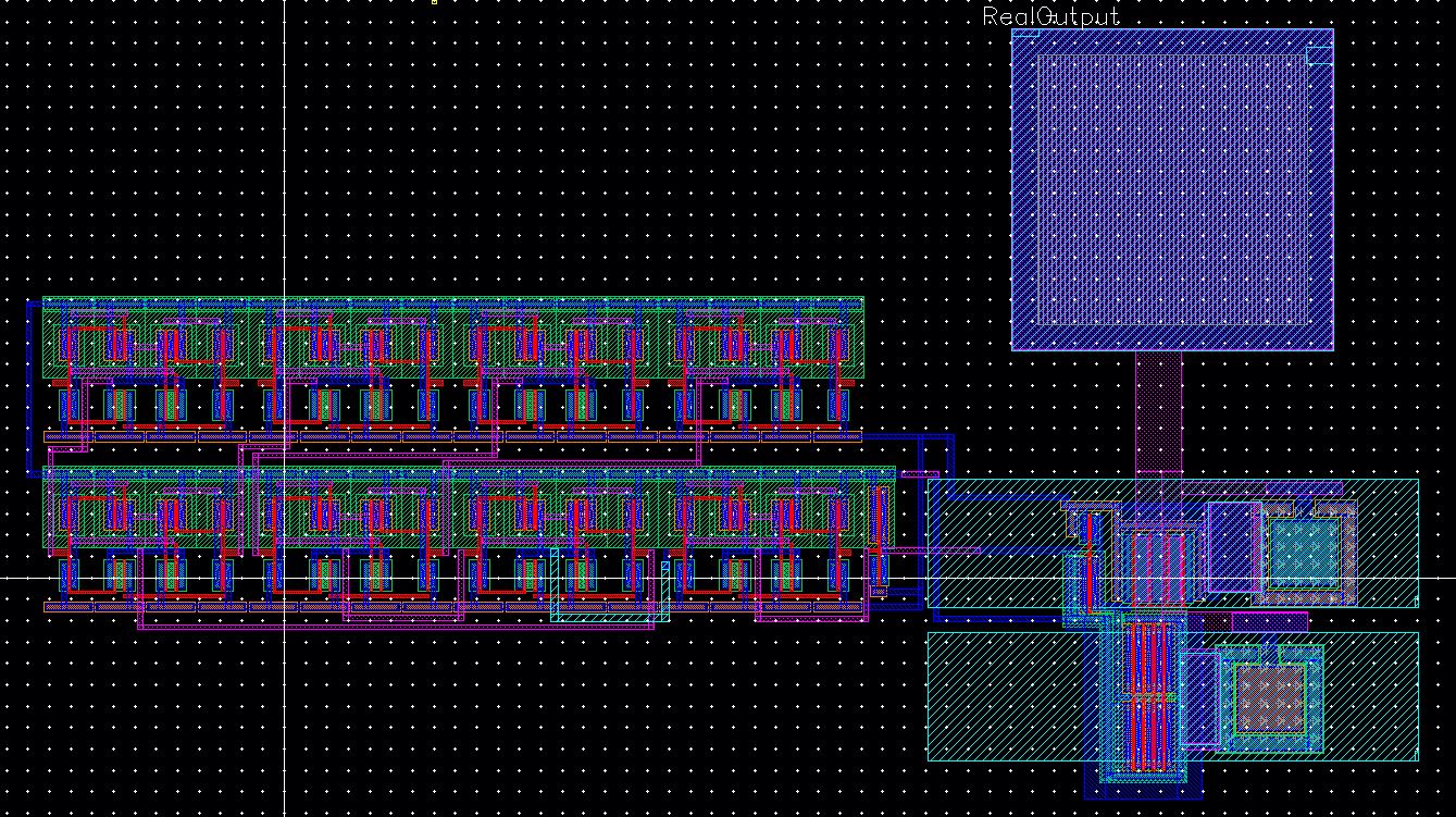 | 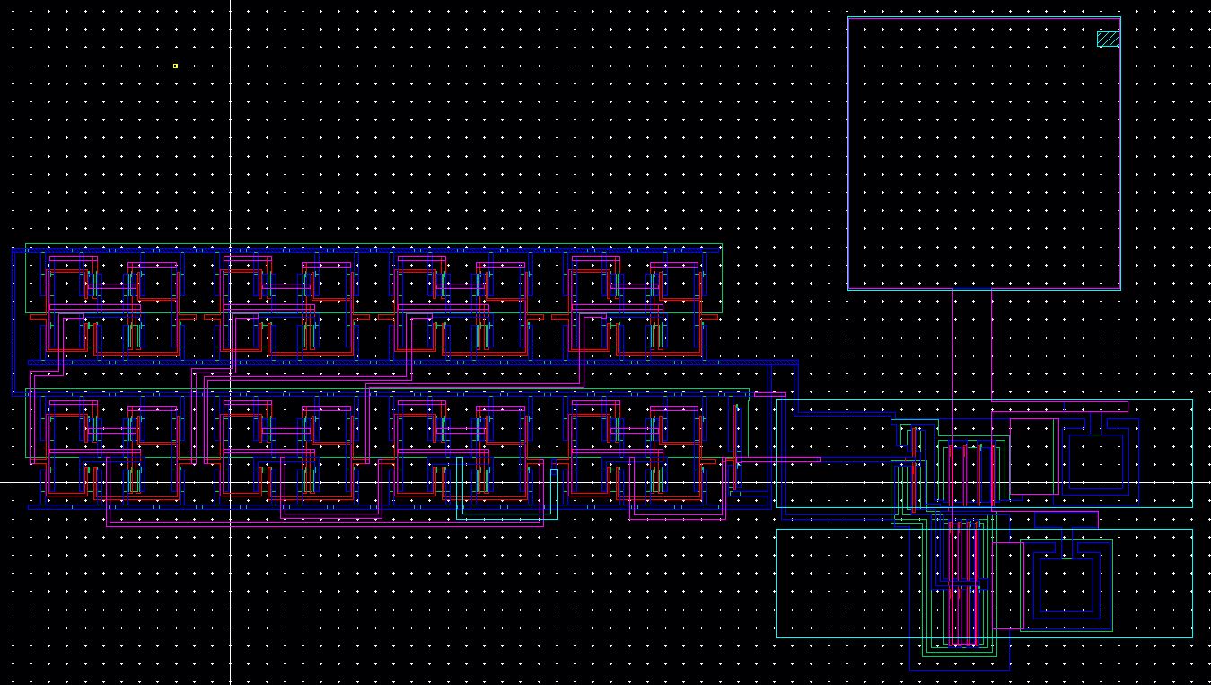 |
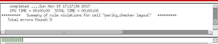
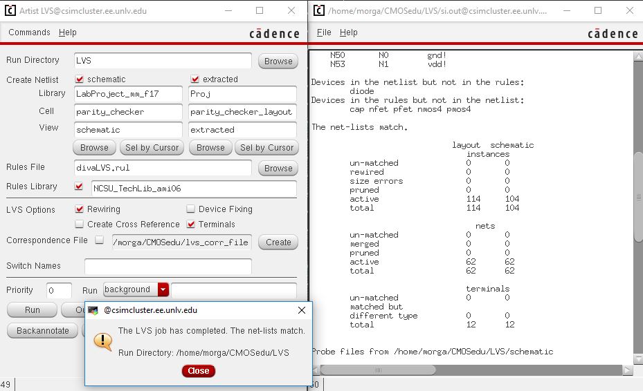
| DRC | LVS |
 |  |
| Simulation Schematic | Simulation |
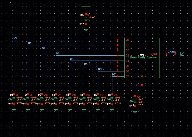 | 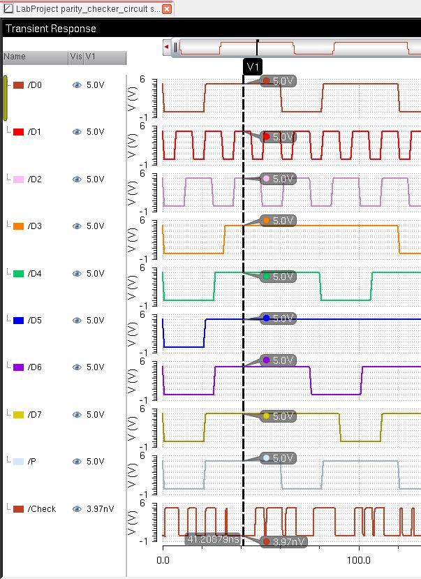 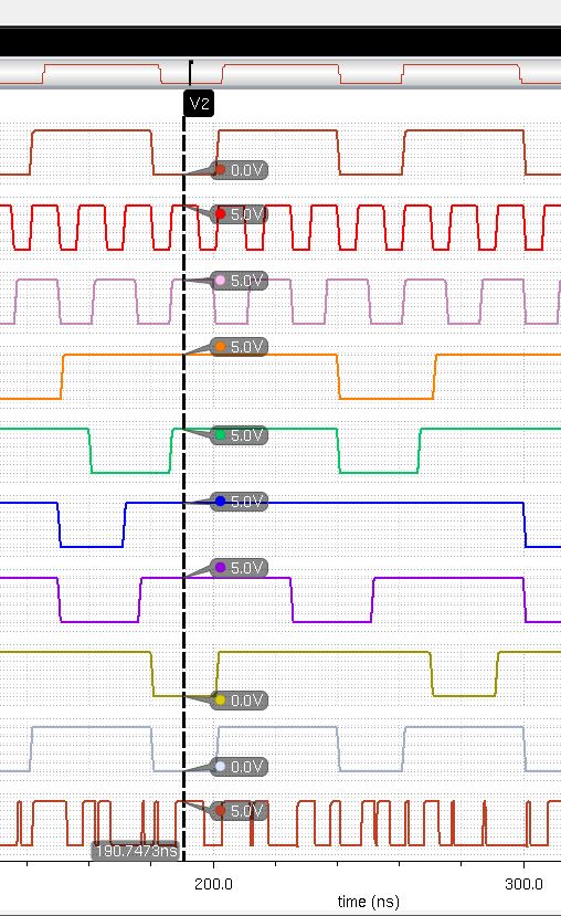 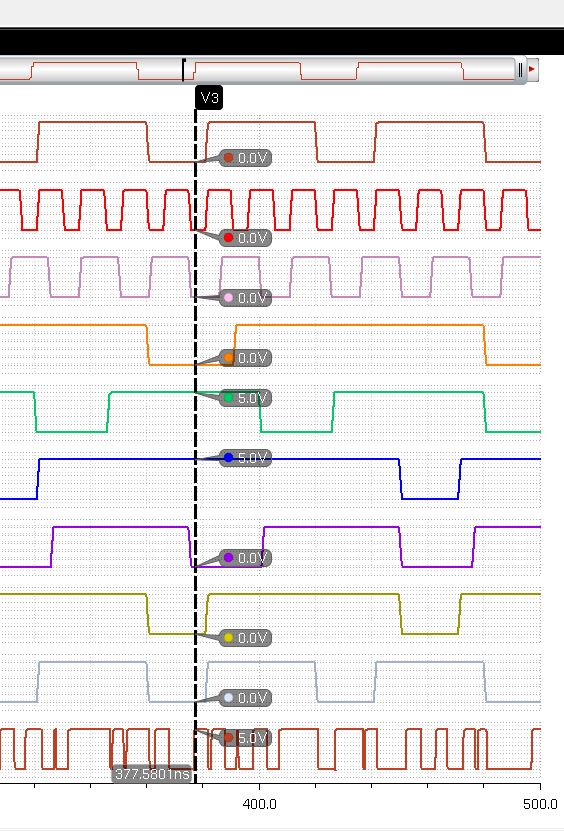 |
I created a simulation schematic with 8-bits, having varying periods and pulse widths. The varying pulse widths and periods made it easier for me to see the outputs at a certain point of the simulation. The simulation above shows varying results with different input bits:
| [Check@V1] = (D0=1,D1=1,D2=1,D3=1,D4=1,D5=1,D6=1,D7=1,P=1) = 0 {9 Odd amount of bits including Parity bit} [Check@V2] = (D0=0,D1=1,D2=1,D3=1,D4=1,D5=1,D6=1,D7=0,P=0) = 1 {6 Even amount of bits including Parity bit} [Check@V3] = (D0=0,D1=0,D2=0,D3=0,D4=1,D5=1,D6=0,D7=0,P=0) = 1 {2 Even amount of bits including Parity bit} |
Link to Lab Directory LabProject_mm_f17
Return to Miguel's Labs
Return to EE 421L Labs