Lab 7 - EE 421L
Authored
by Miguel Morga,
November 6, 2017
morga@unlv.nevada.edu
Prelab:
The
prelab required us to back up all of our course work as usual, so i did
this on my student drive. It was also required for us to go through
Tutorial 5, and to read the entire lab before starting it.
Lab Report:
Inverter:
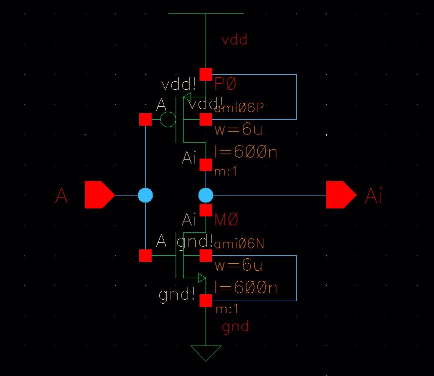
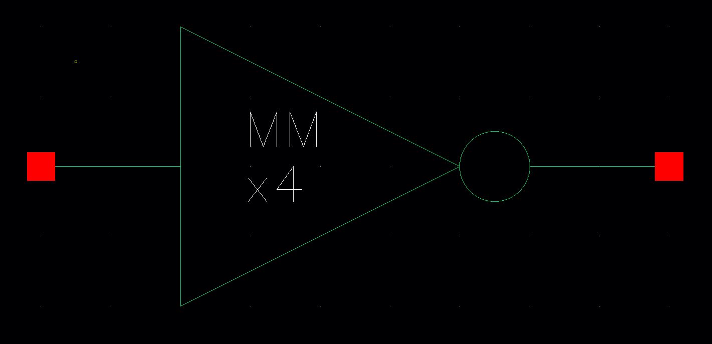
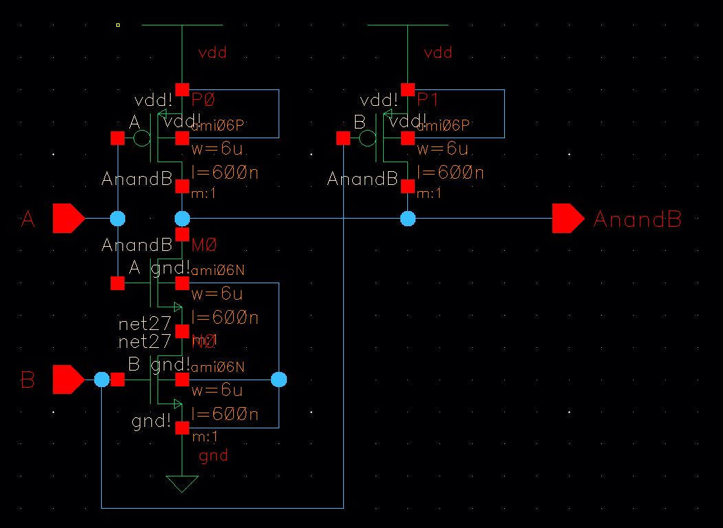
I created an inverter using an NMOS and a PMOS, then a simple symbol was made for it.
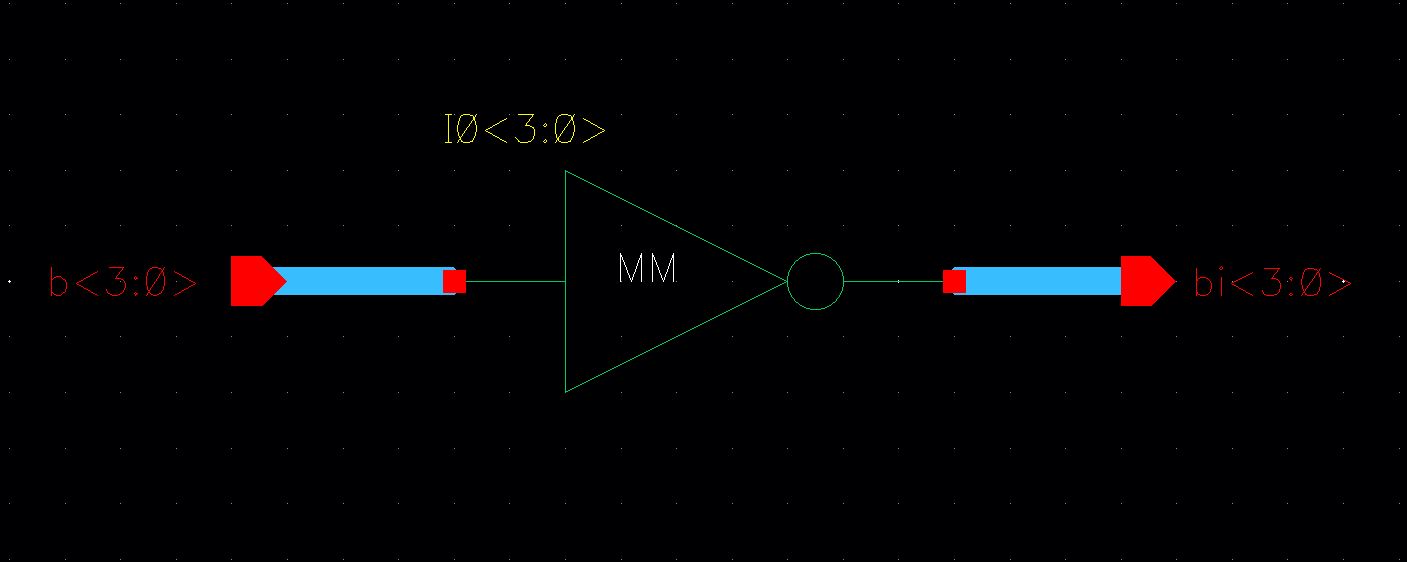
To create an equivalent, more concise schematic I used and array name
of IO<3:0>. Thejn I connected a bus to the input and output pins
of the inverter from which we learned how to do in the tutorial.
| Schematic | Symbol | Concise Schematic |
 |  |  |
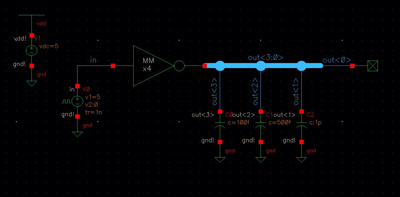
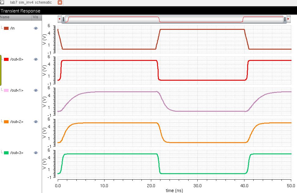
Now
that I had the symbol for my inverter I created the simulation
schematic below. All four of the inputs are tied together to an input
pulse source while the outputs are connected to different capacitors.
Simulating the schematic gave me the waveforms below.
| Simulation Schematic | Simulation |
 | 
|
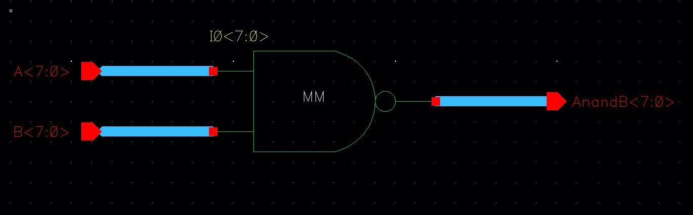
NAND:
The
same process was made for a NAND gate as was done with the inverter.
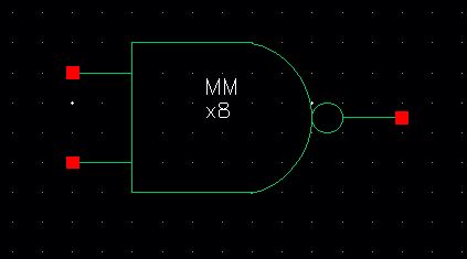
The only difference is that the process had to be done with an 8-bit
input/output NAND gate.
| Schematic | Symbol | Concise Schematic |
 |  |  |
| Simulation Schematic | Simulation |
| 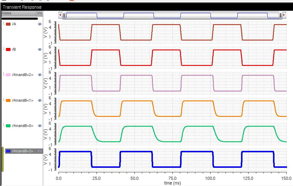
|
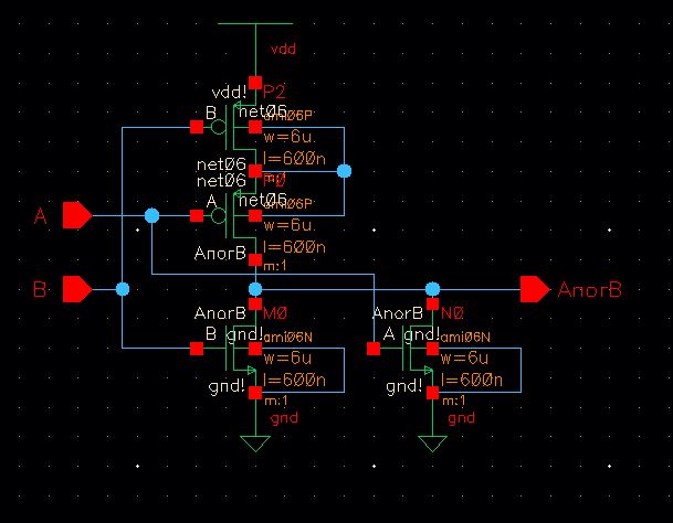
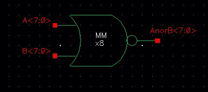
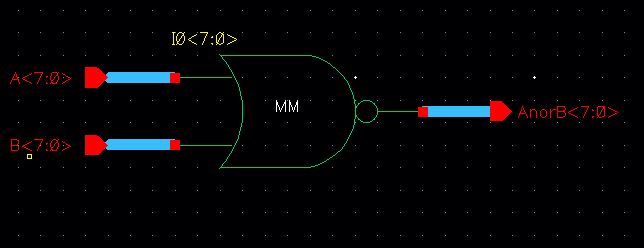
NOR:
The same process was made for a NOR gate as was done with the NAND gate.| Schematic | Symbol | Concise Schematic |
| 
| 
|
| Simulation Schematic | Simulation |
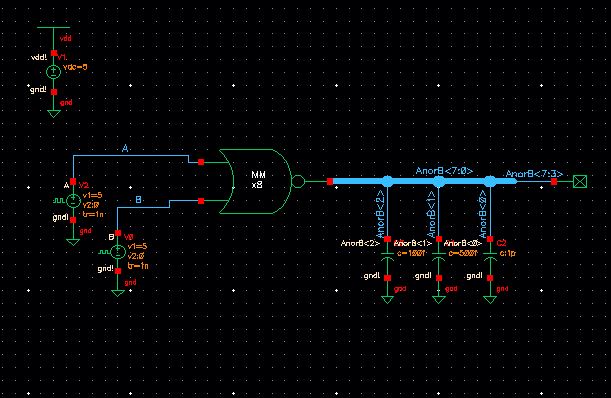
| 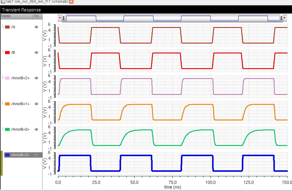 |
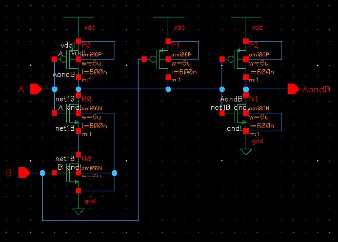
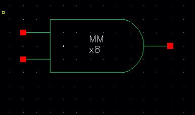
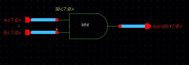
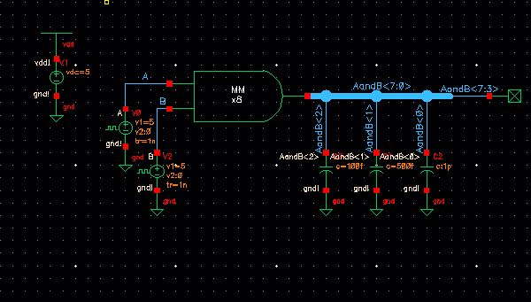
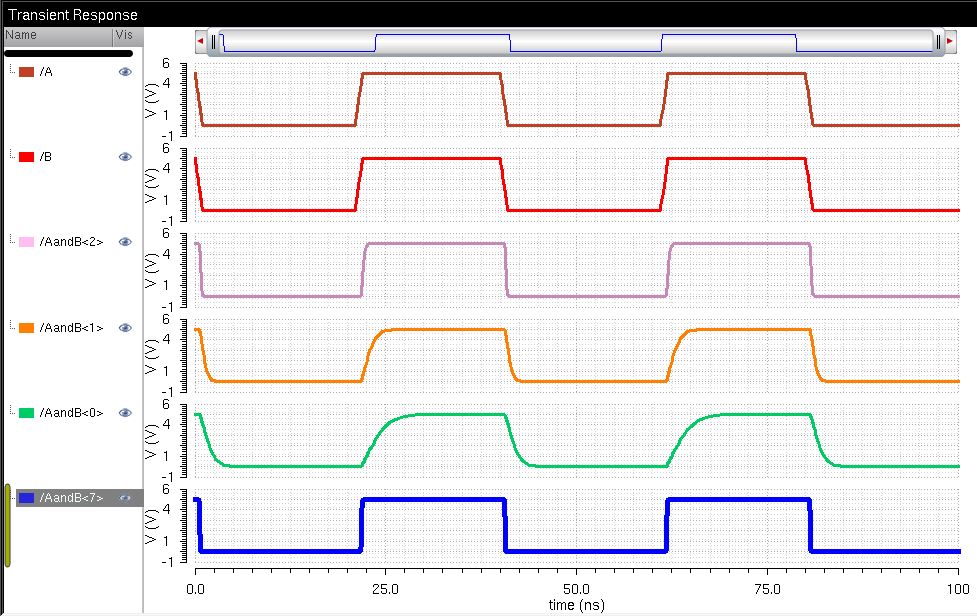
AND:
The same process was made for a AND gate as was done with the NOR gate.| Schematic | Symbol | Concise Schematic |
| 
| 
|
| Simulation Schematic | Simulation |
| 
|
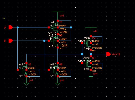
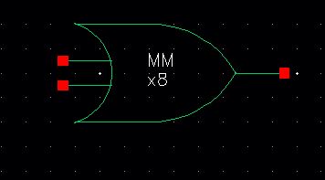
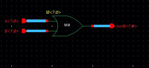
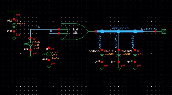
OR:
The same process was made for a OR gate as was done with the AND gate.| Schematic | Symbol | Concise Schematic |
| 
| 
|
| Simulation Schematic | Simulation |
| 
|
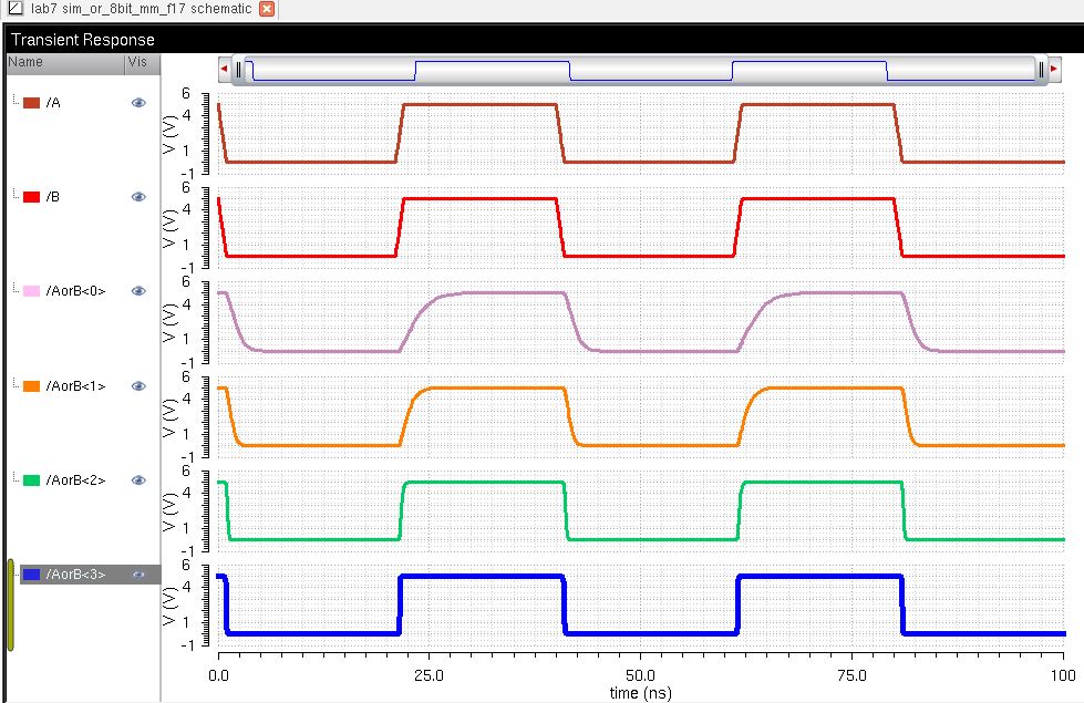
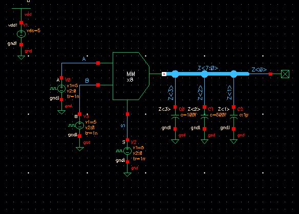
2-to-1 DEMUX/MUX:
The
same as above was required for a 2-to-1 DEMUX/MUX and an 8-bit
DEMUX/MUX. The schematics were created first, followed by a simple
symbol and then a simulation schematic to make sure it functions
properly.
| Schematic | Symbol | Simulation Schematic | Simulation |
| 
| 
|  |
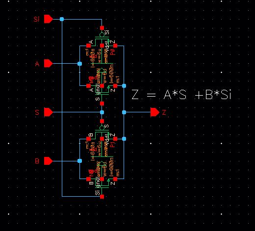
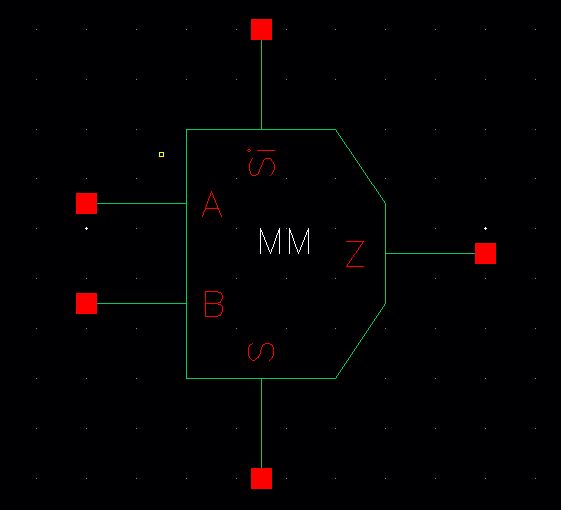
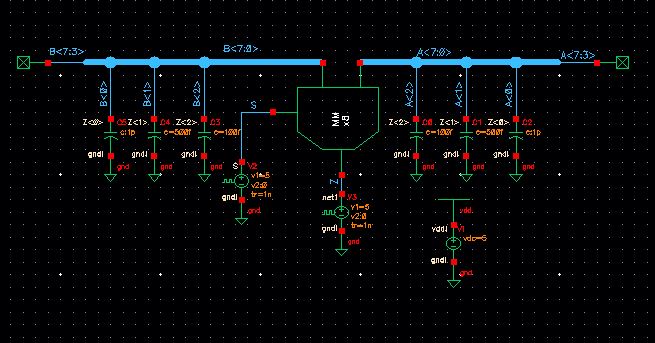
8-bit DEMUX/MUX:
In
order for the concise schematic to be made for the 8-bit DEMUX/MUX an
inverter had to be placed so the cell only needs one select input. This
allows 2 inputs, S and Si, one of them is generated by the inverter.
| Schematic | Symbol | Concise Schematic |
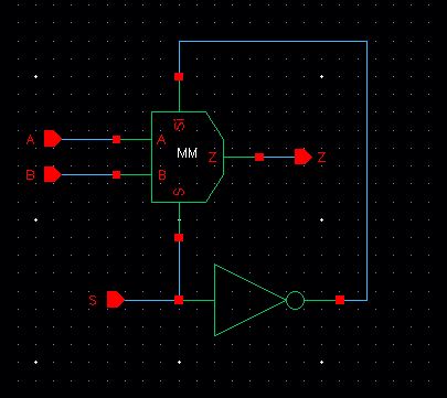
| 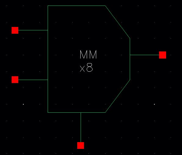
| 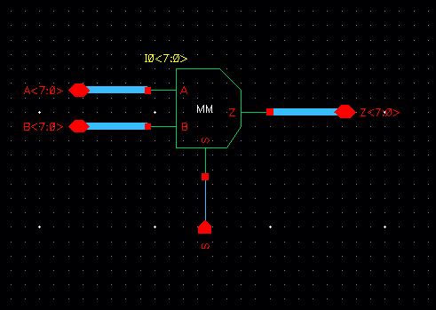
|
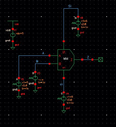
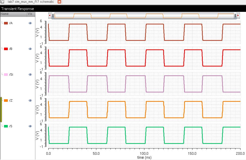
DEMUX/MUX:
The
circuit can be used for both multiplexing and demultiplexing. This can
be done since it is basically the same process just reversed. For the
MUX we have two inputs and for the DEMUX we have 2 outputs which should
have been the inputs on the MUX.
| Simulation Schematic | Simulation |
| 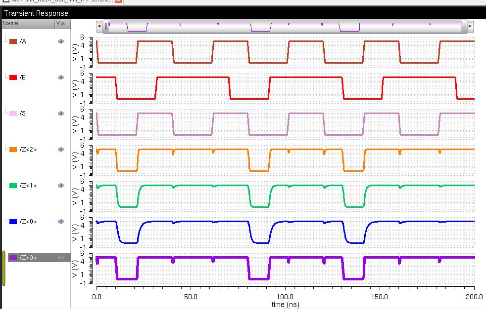 |
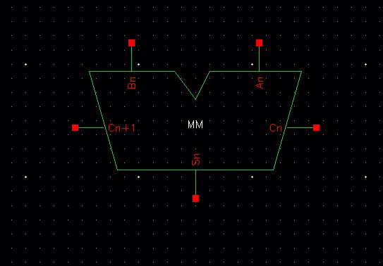
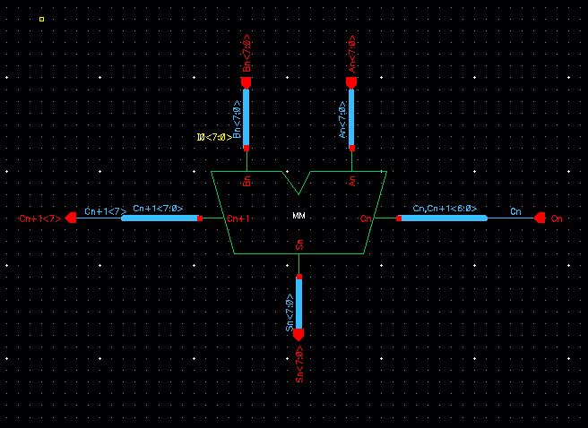
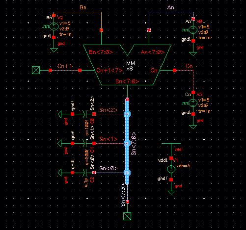
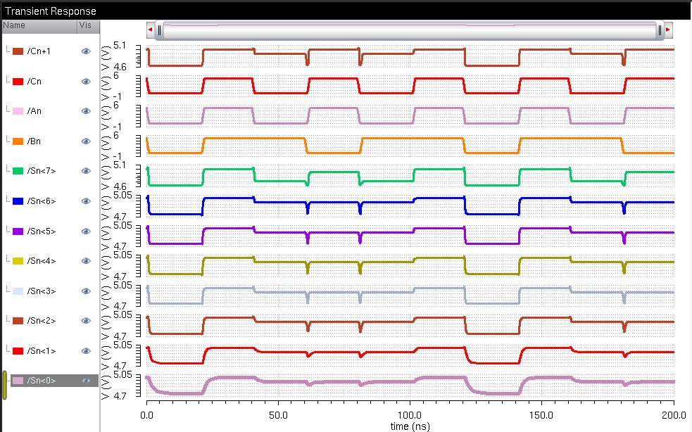
Full Adder:
| Schematic | Symbol | Concise Schematic |
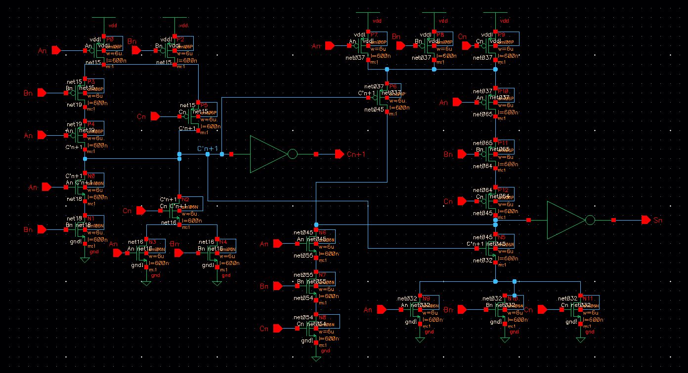 |  |  |
| Simulation Schematic | Simulation |
 |  |
| Layout | Extracted |
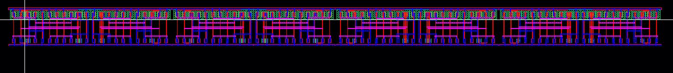 | 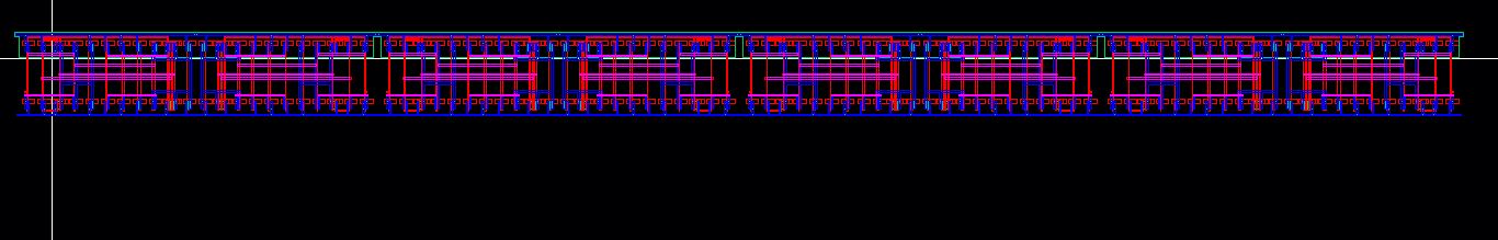 |
Link to Lab Directory lab7_mm_f17
Return to Miguel's Labs
Return to EE 421L Labs