Lab 6 - EE 421L
For our prelab we had to back up all of our previous work like how weve been doing in our other labs. Then i went through the tutorial 4 in Cadence entirely that was refenced in the lab instructions.
| Symbol | Schematic |
 |  |
| Layout | Extracted |
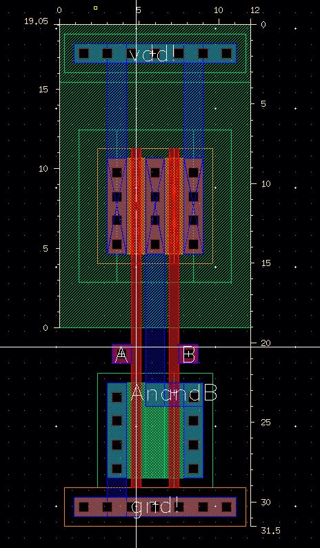 | 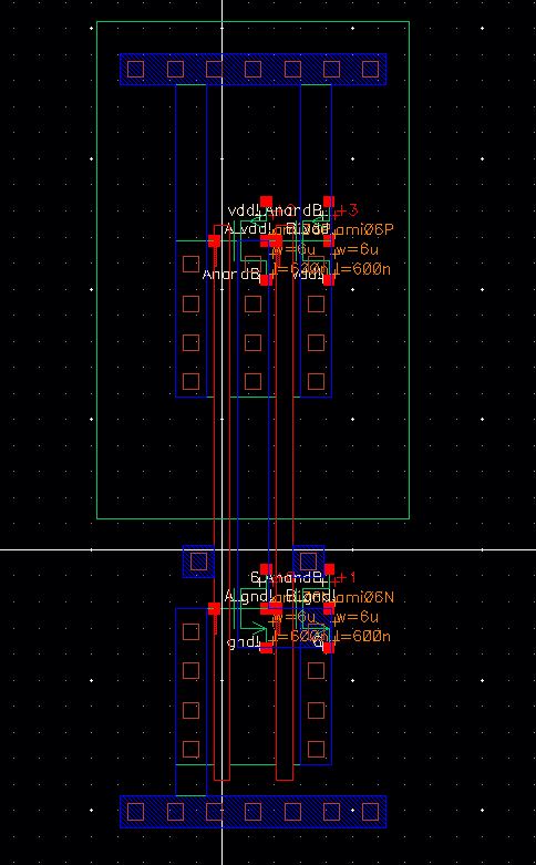 |
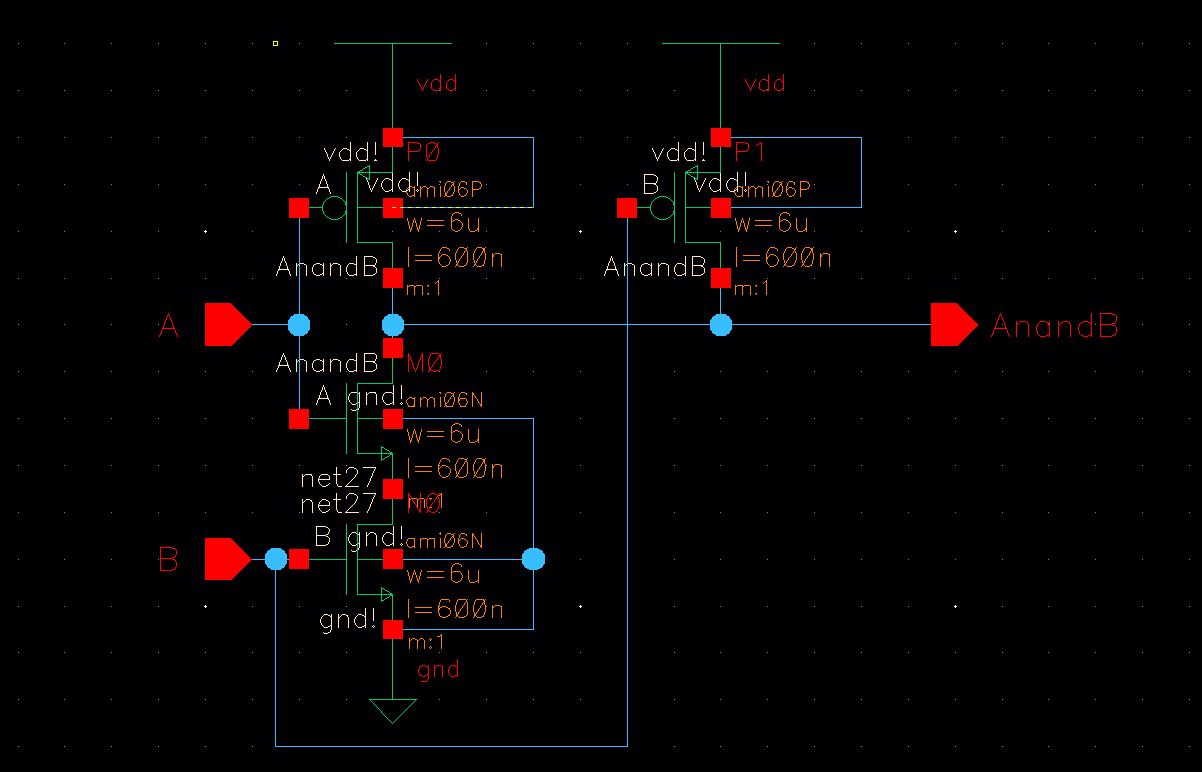
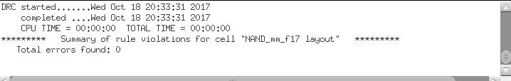
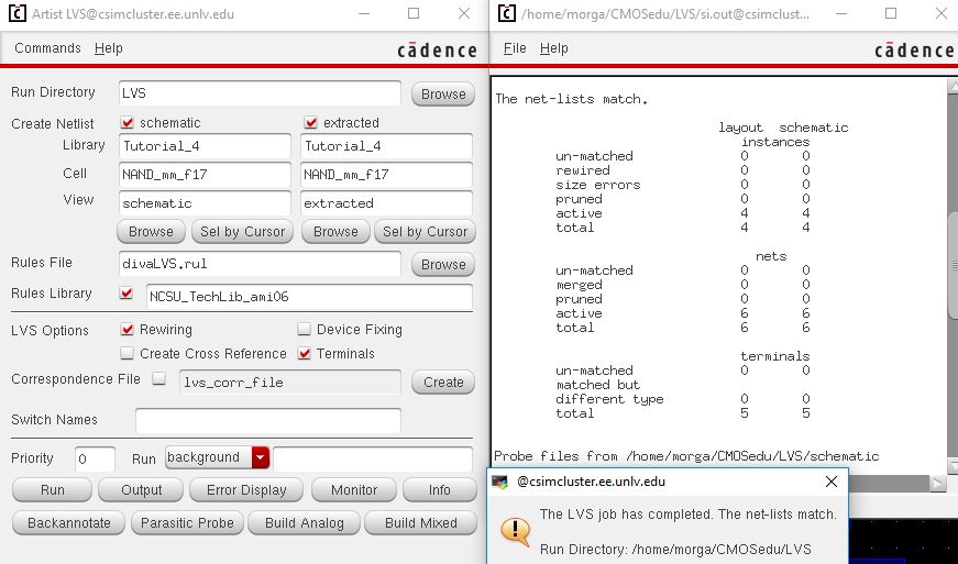
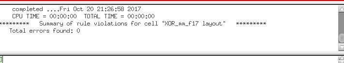
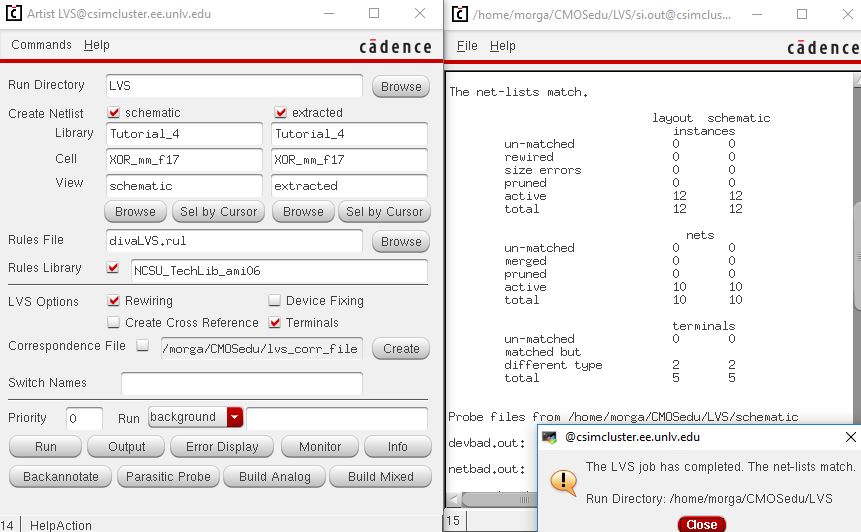
In the images below it can be seen that the cells I created DRC'd and LVS'd without any issues in the end.
  |
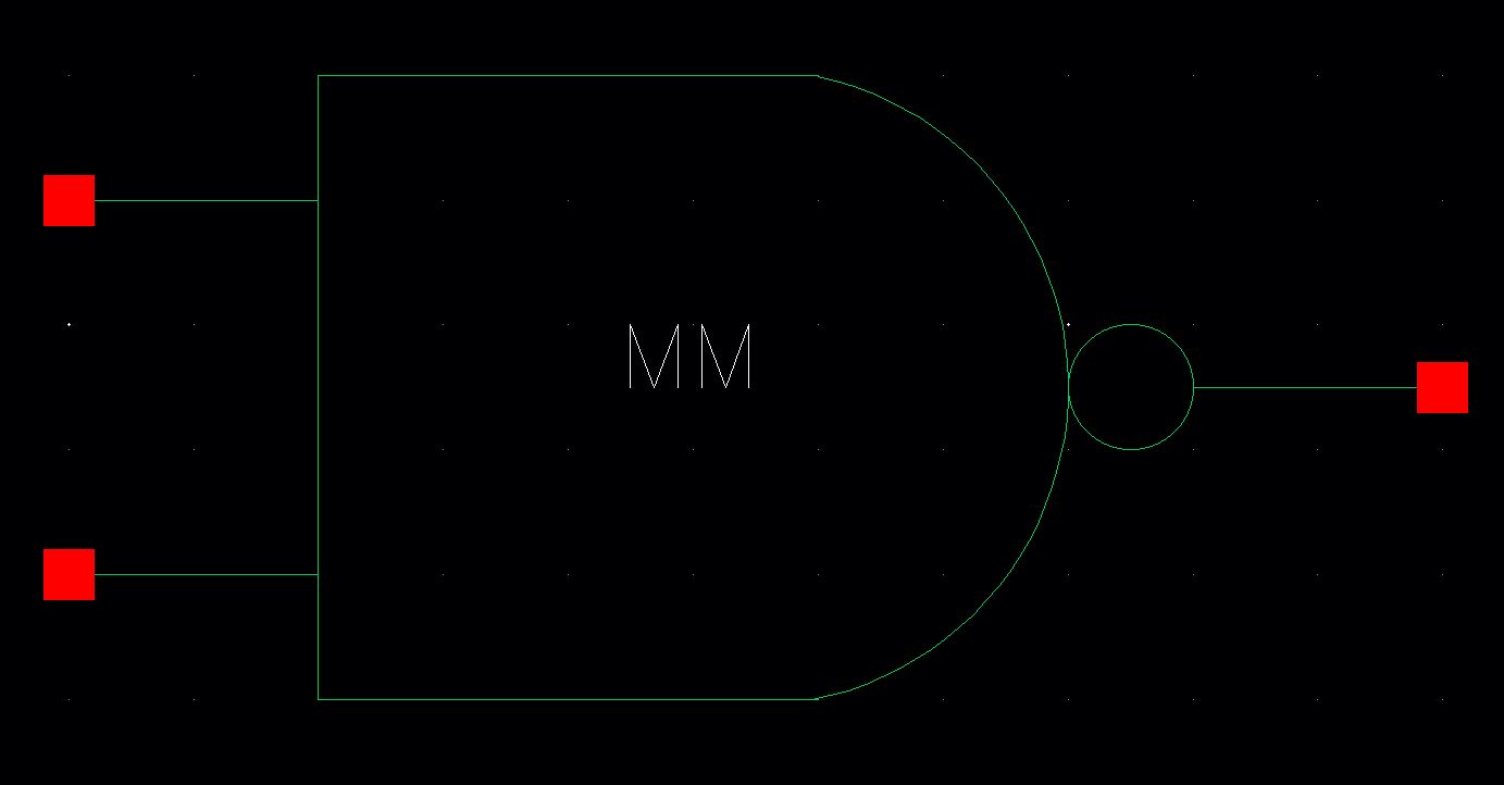
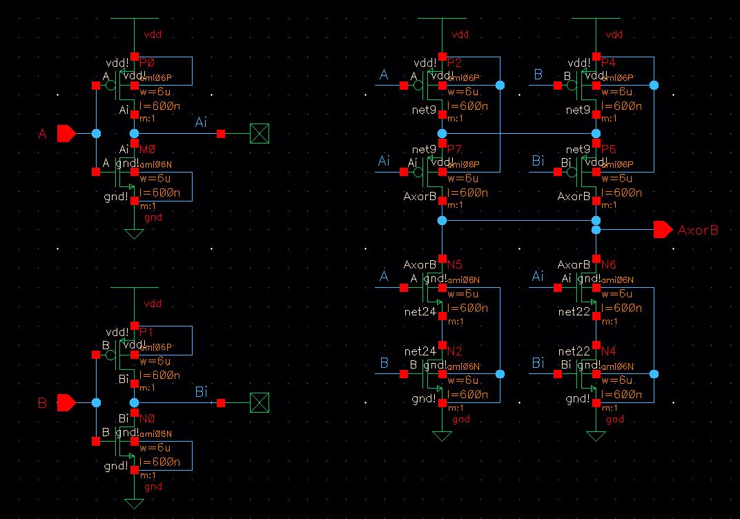
2 Input XOR gate:
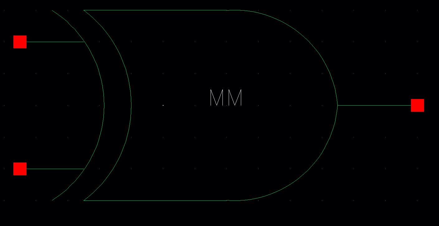
The 2 input XOR gate was created using 6u/0.6u MOSFETS. To create the symbol I designed it to look like an actual xor gate and not just boxes like we normally do and slapped my initials on it as well.| Symbol | Schematic |
 |  |
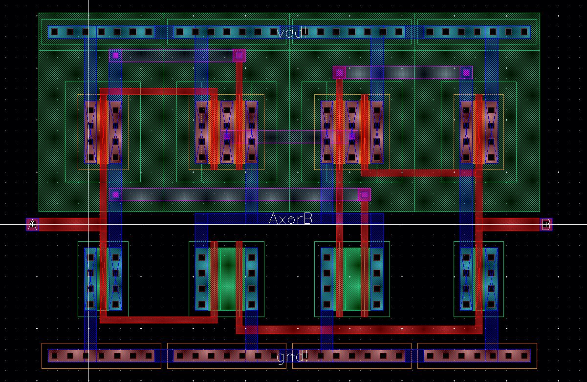
For the xor layout I did the same with the standard cell frames as I did on the nand gate layout. I made them all the same height and gave some room in each frame to route wires in between.
| Layout | Extracted |
 | 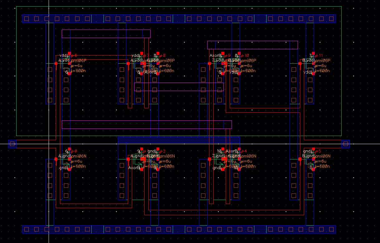 |
The cells I created for the xor gate also DRC'd and LVS'd properly.
  |
Gate Simulation:
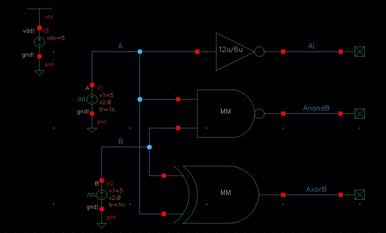
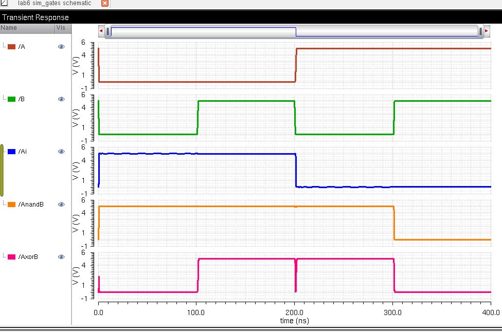
I created the schematic below with the gates I created previosly in the lab and an inverter. This was created to test the logical operation of the gates for all 4 possible inputs (being 00 01 10 11).
| Schematic | Simulation |
 |  |
Full Adder:
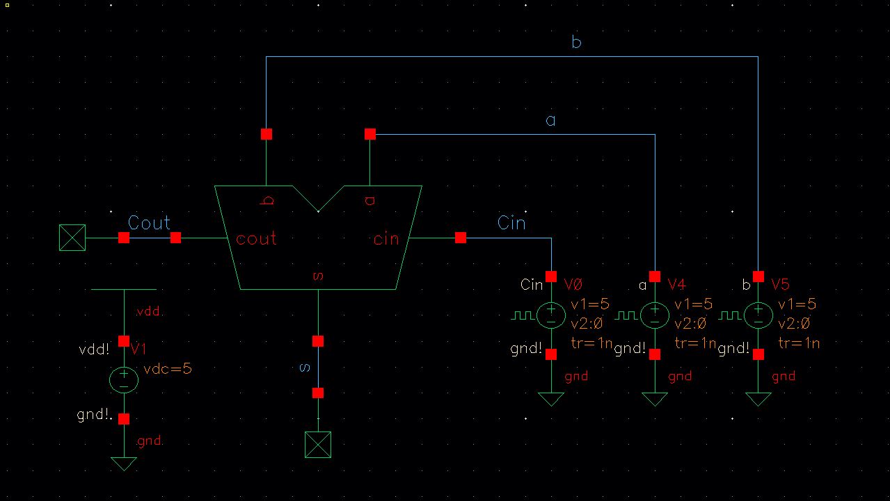
It was then required to draft a full adder with what we've created in the lab so far. So 3 nand gates and 2 xor gates were used.
| Schematic | Symbol |
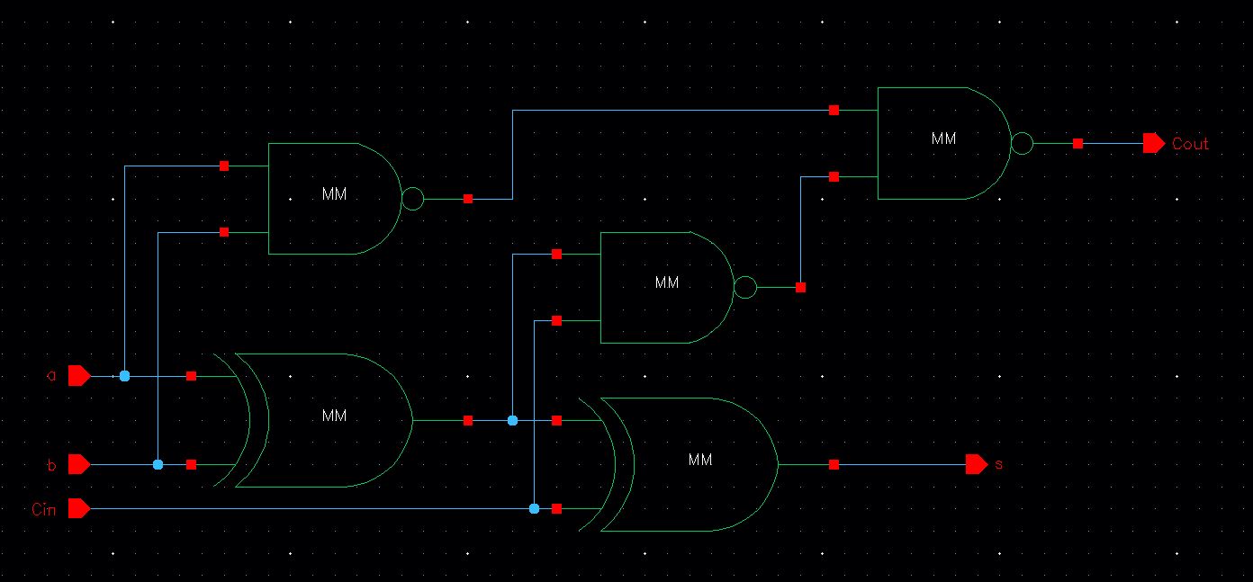 | 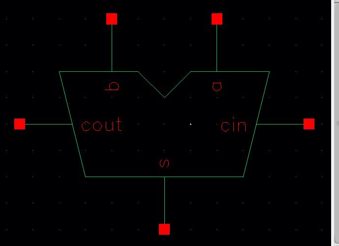 |
The layout was then created and this is where the use of standard cell frames came in handy. I snapped the groups of nand gates together and seperated the xor gates for ease of wiring. The cell frames made it easier for wires not to overlap or touch and make them more visible as well.
| Layout | Extracted |
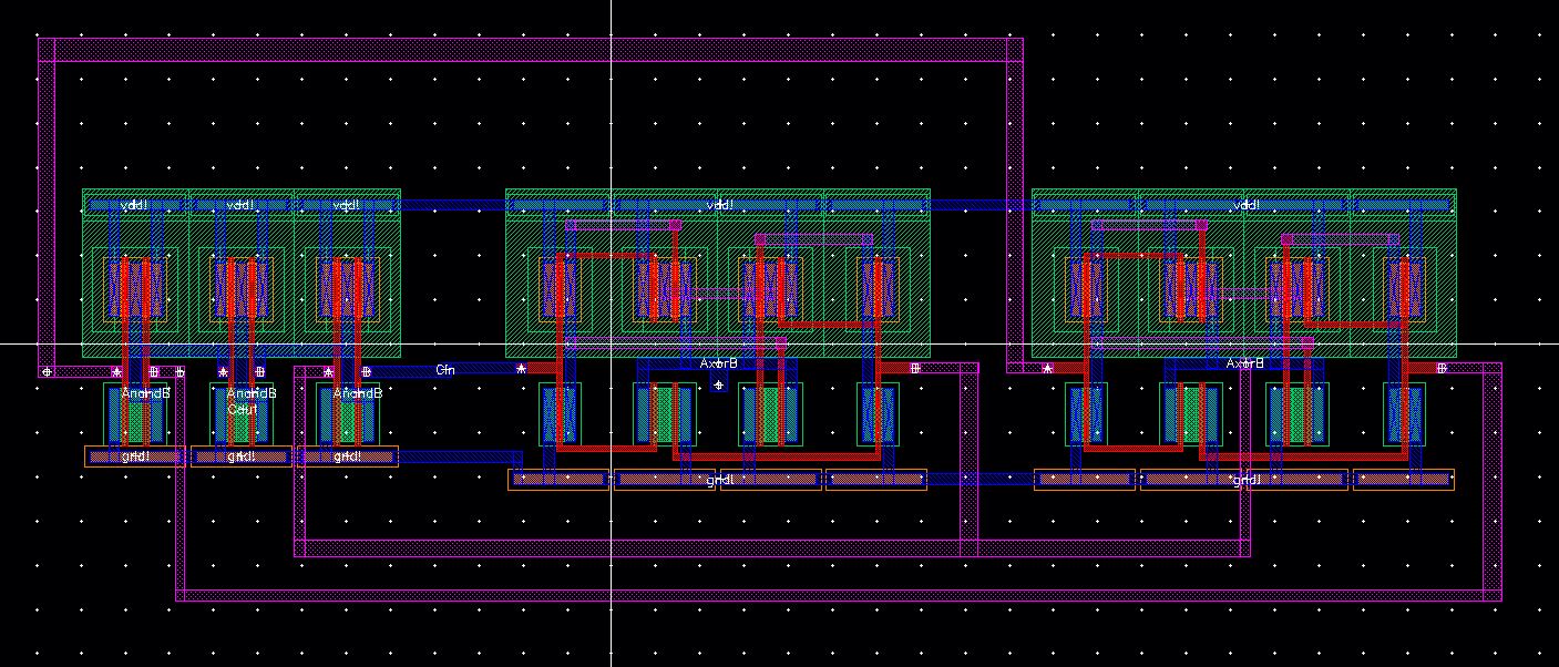 | 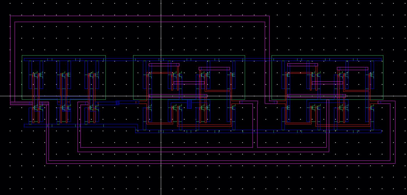 |
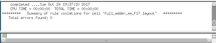
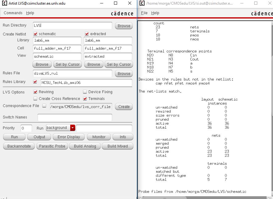
After completing the layout and fixing a few wiring problems the cells DRC'd and LVS'd fine.
  |
| Schematic | Simulation |
 | 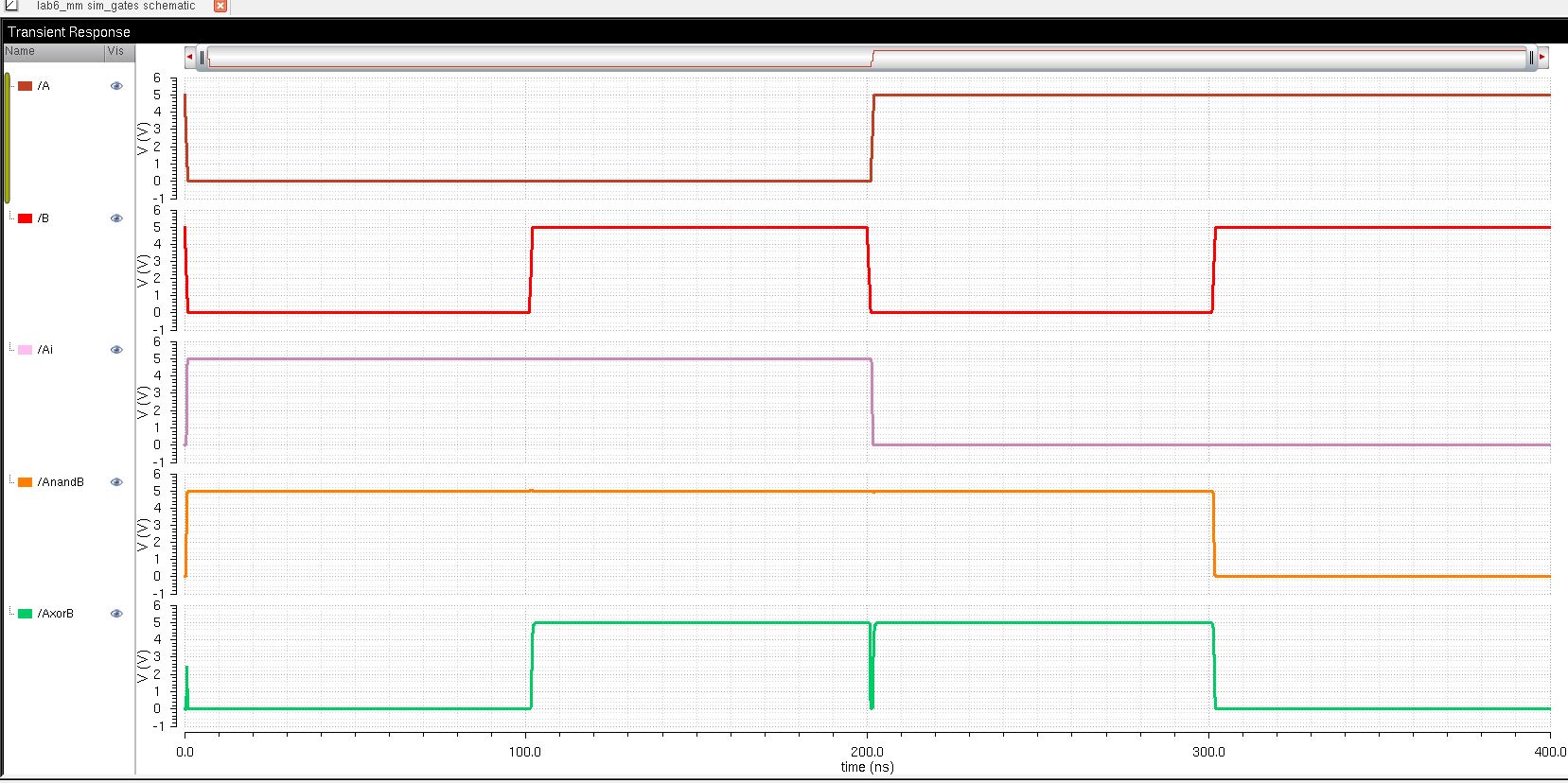 |
In the 2 simulations above it can be seen that the xor gate is glitching. This is because the inputs are changing simultaneously but the rise and fall time are not changing at the exact same time, there is a delay. This can possibly be fixed if the delay was smaller.
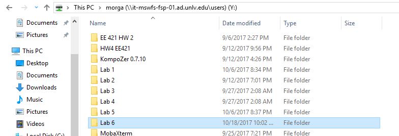
Link to my file directory lab6_mm