Lab 5 - EE 421L
To start off the laboratory it was required to go over the Tutorial
3 to understand how to design, layout and simulate a CMOS inverter. After
this I backed up my work onto my student drive and onto my usb flash drive.
|
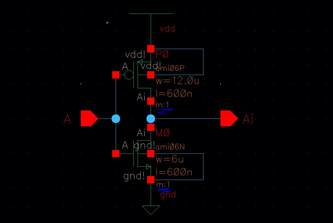
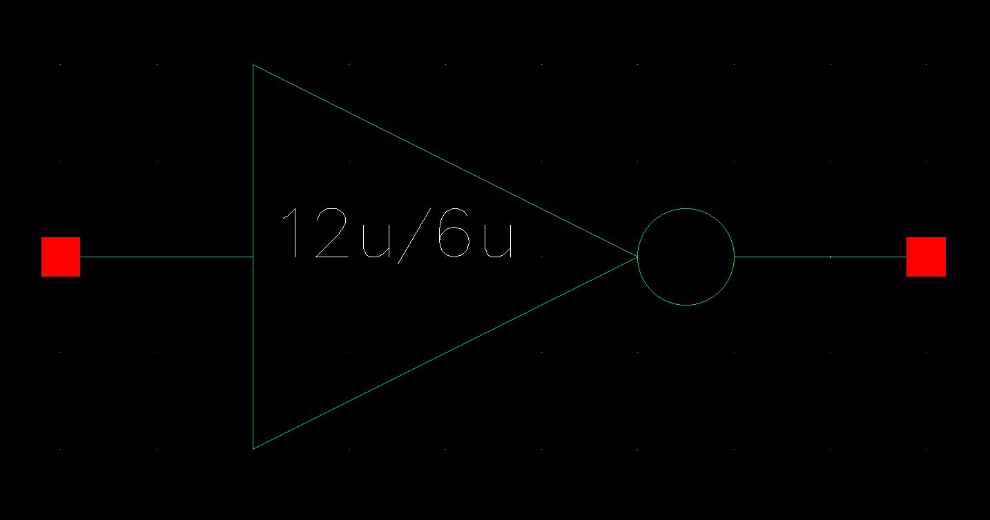
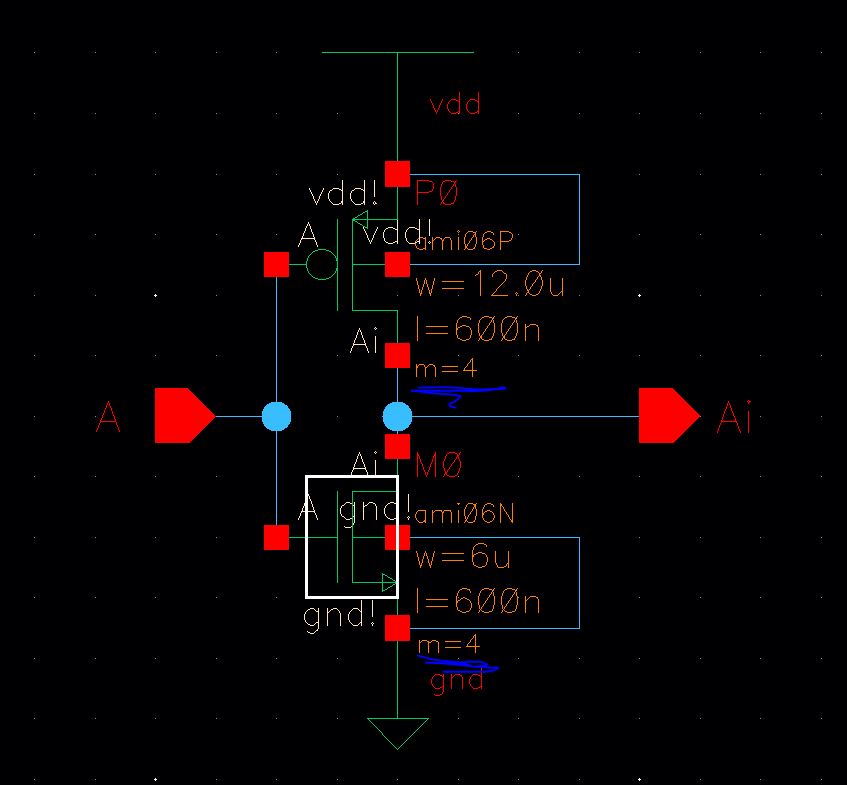
Below is the schematic and the symbol I created for the 12u/6u
inverter. The 12u/6u is equal to the width of the PMOS / the width of the NMOS,
and both devices in the circuit have a minimum length of 0.6u.
 |  |
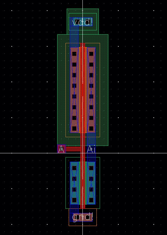
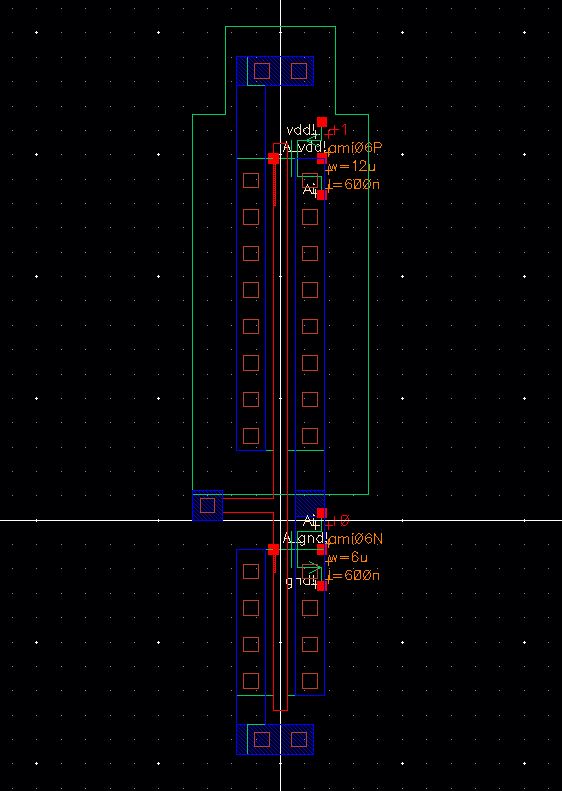
I then created the layout of the 12u/6u inverter. The power
is connected to the top of the cell/n-well via metal1 using the ntap cell.
Ground is connected to the bottom of the cell/p-substrate via metal1 using the
ptap cell. I used a single row of contacts to reduce layout size. The schematic
has an input pin (A), output pin (Ai), vdd!, and gnd! I drafted it by following
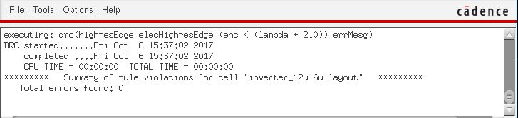
the steps in Tutorial 3. Once I completed the layout, I DRC's it to check for
mistakes. No mistakes were found which allowed me to get the extracted layout
of the inverter.
 |
 |
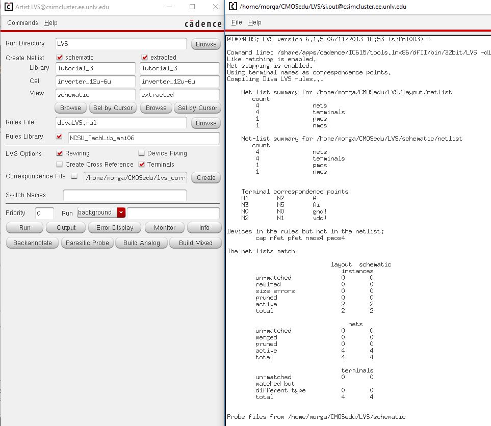
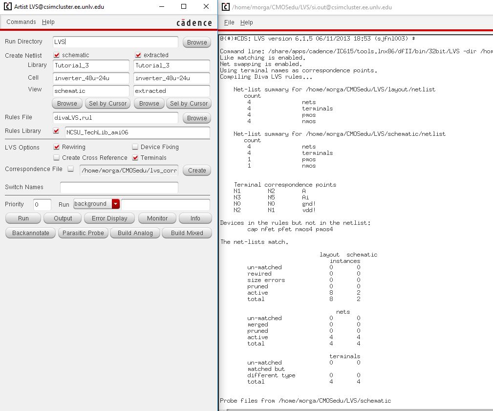
I opened up the extracted layout which allowed me to compare
it to the schematic by the LVS function. I compared both the schematic and the
layout view of the 12u/6u inverter to find that the netlists matched and they
were equal to one another.
 |  |
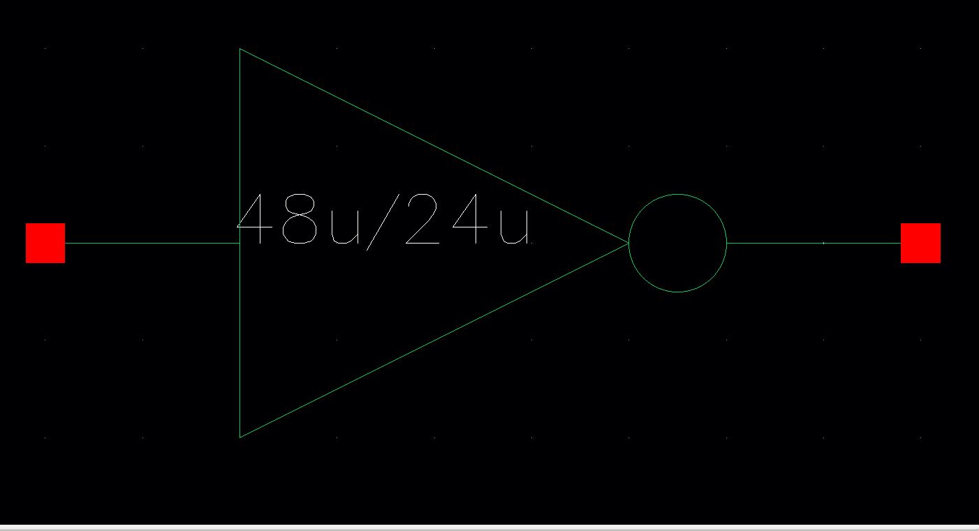
48u/24u Inverter:
Below is the schematic and the symbol I created for the
48u/24u inverter. The 48u/24u is equal to the width of the PMOS / the width of
the NMOS. This is basically exactly the same as the 12u/6u inverter but it has
a multiplier (underlined in blue in the schematic) which sets the inverter to
be equivalent to a 48u/24u inverter.
 |  |
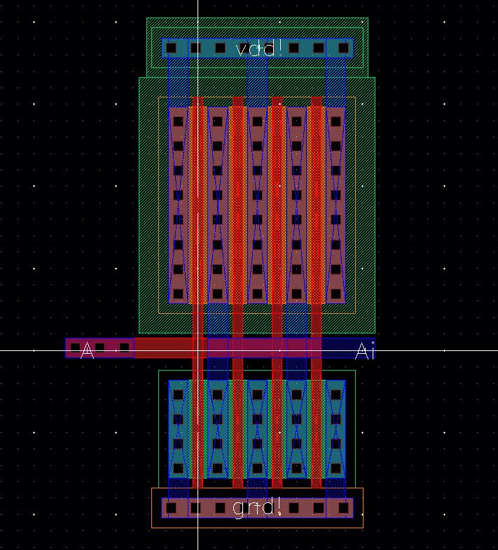
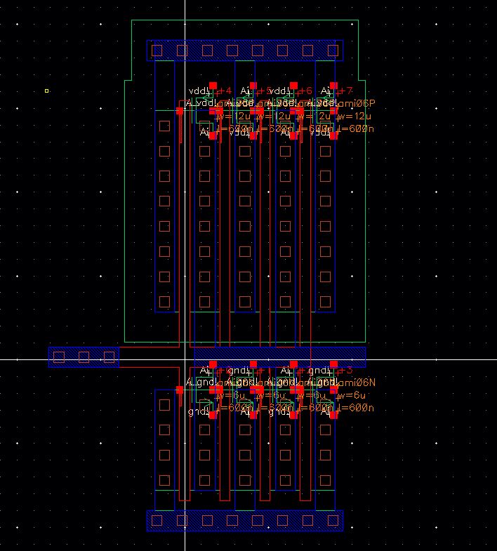
I then created the layout of the 48u/24u inverter. To design
this layout I just used the multiplier of 4 for each part of the 12u/6u
inverter which increased the size of the ntaps, ptaps, nmos, pmos, and m1_poly.
The power is connected to the top of the cell/n-well via metal1 using the ntap
cell. Ground is connected to the bottom of the cell/p-substrate via metal1
using the ptap cell. I used a single row of contacts to reduce layout size. The
schematic has an input pin (A), output pin (Ai), vdd!, and gnd!. Once I
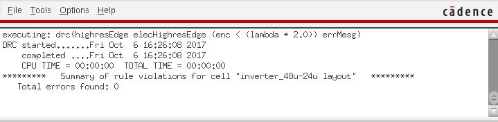
completed the layout, I DRC's it to check for mistakes. No mistakes were found
which allowed me to get the extracted layout of the inverter.
 |
 |
To simulate the operation of the 12u/6u inverter I created 4
separate circuits with different capacitive loads and allowed the SPICE
programs in CADENCE to show the results. I adjusted the settings to what was
required in the laboratory. These settings were applied to the SPECTRE and
UltraSim simulation programs which resulted in the graphs below. Both SPECTRE
and UltraSim simulations came out just about exactly the same. By seeing the
results in the graphs I noticed that as the capacitance increases, the output
signal begins to fall. Sure it is different with each different capacitive load
but the inverting is still occurring from the rising edge to the falling edge in
each graph.
| Capacitive Load | Schematic | Spectre Simulation | UltraSim Simulation |
| 1pF | 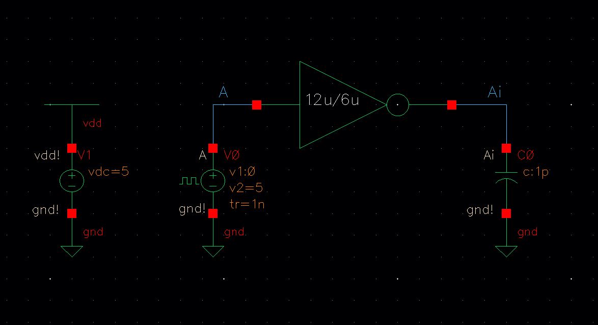 | 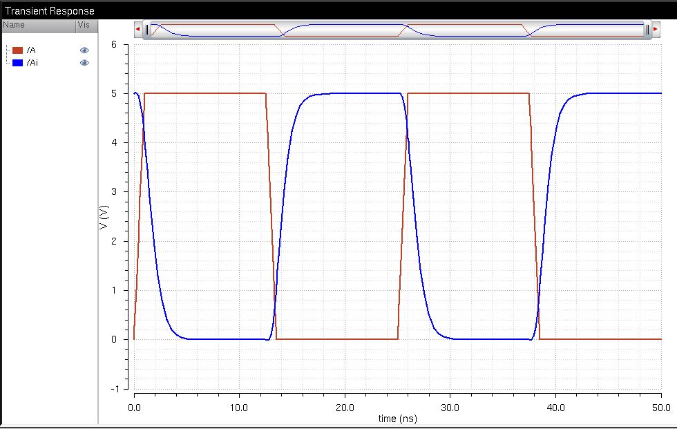 | 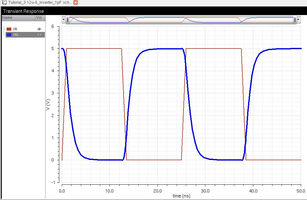 |
| 10pF | 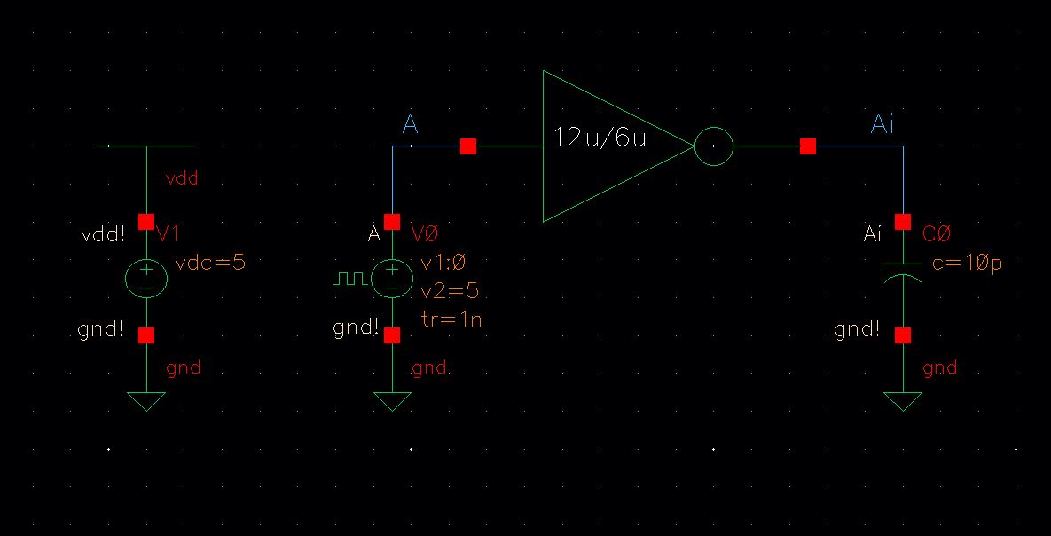 | 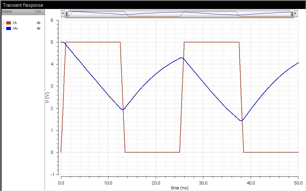 | 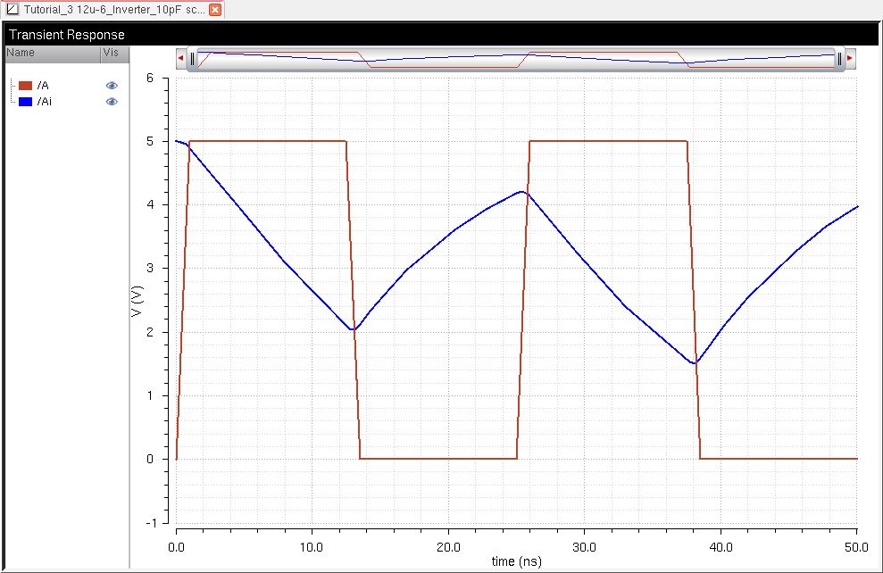 |
| 100pF | 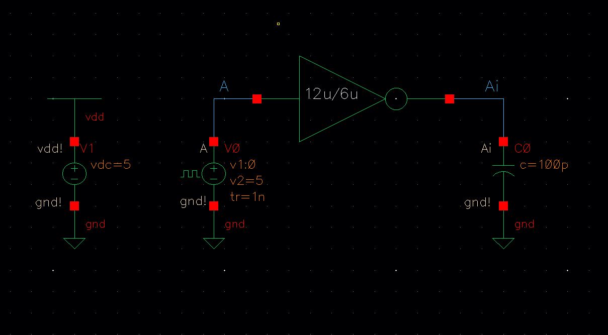 | 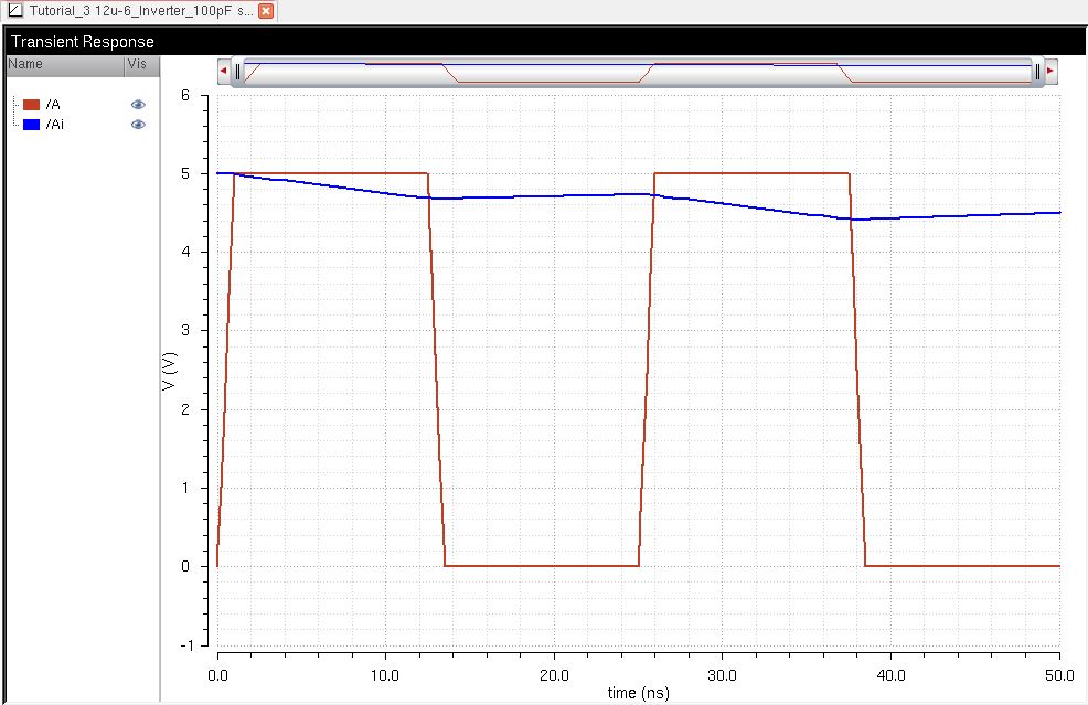 | 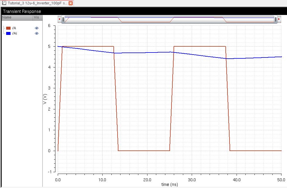 |
| 100fF | 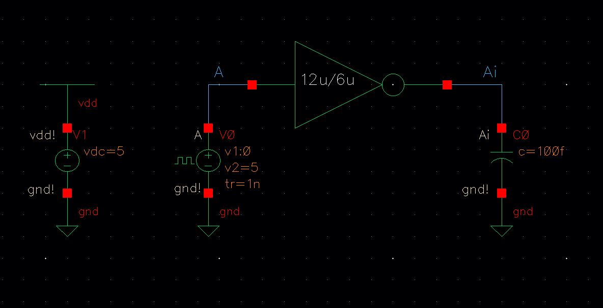 | 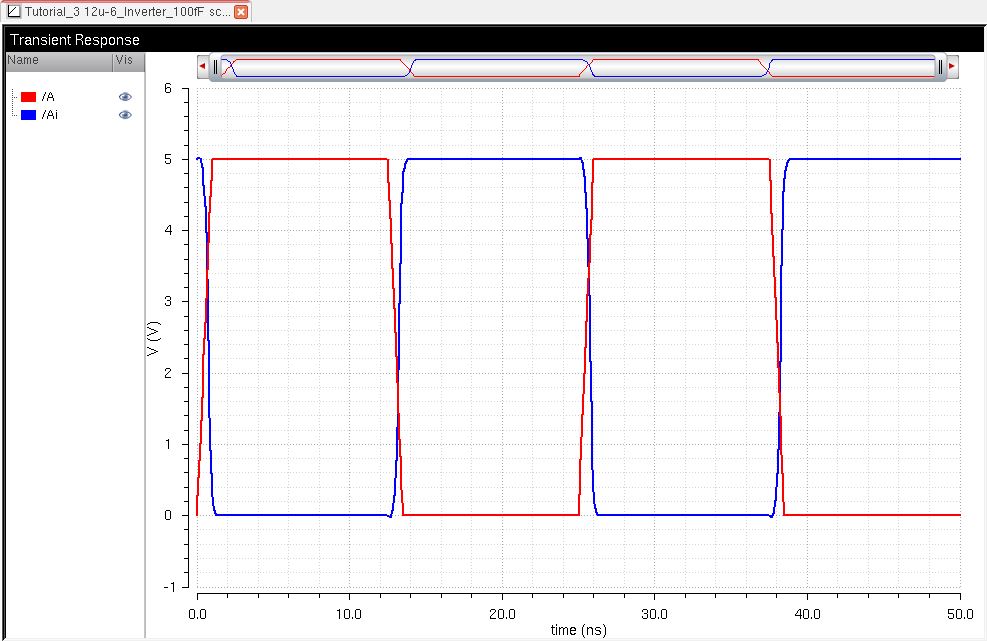 | 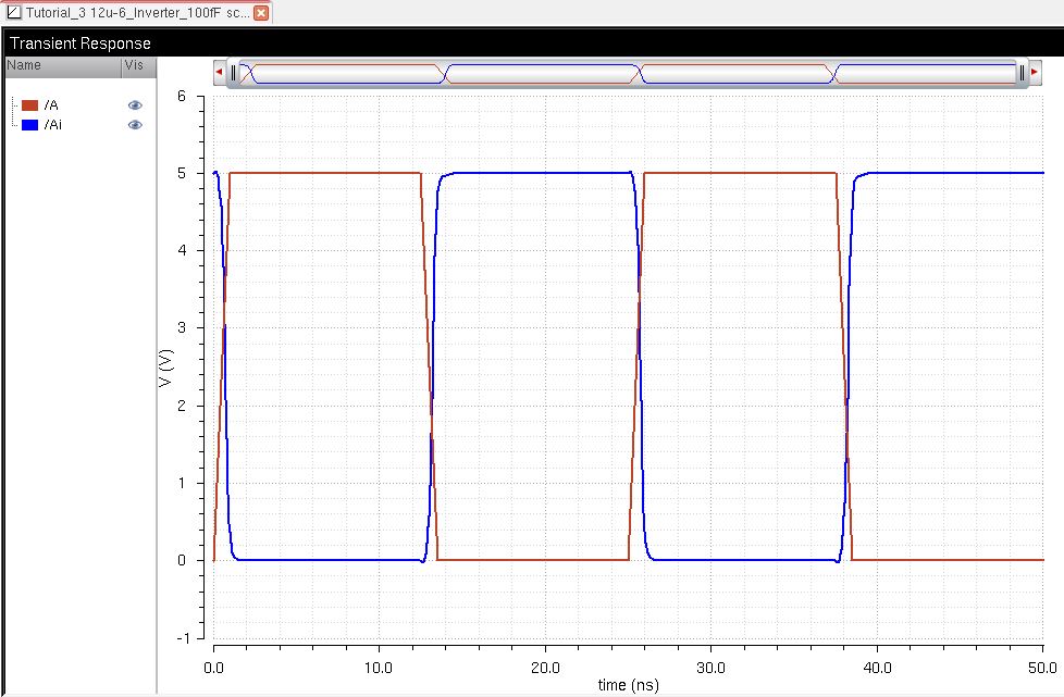 |
| Capacitive Load | Schematic | Spectre Simulation | UltraSim Simulation |
| 1pF | 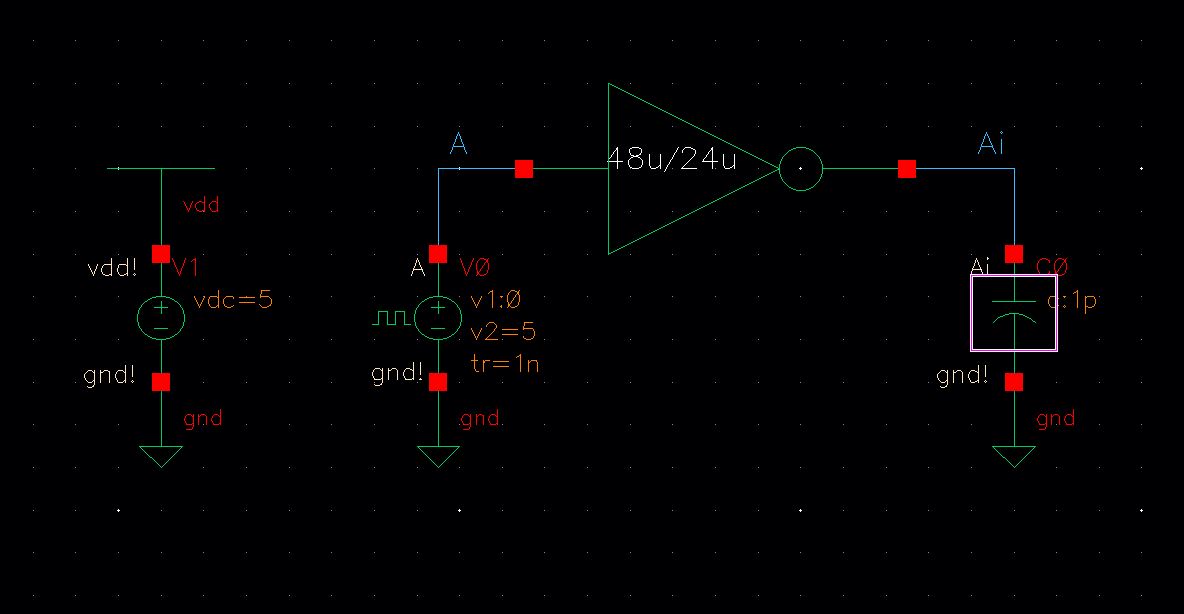 | 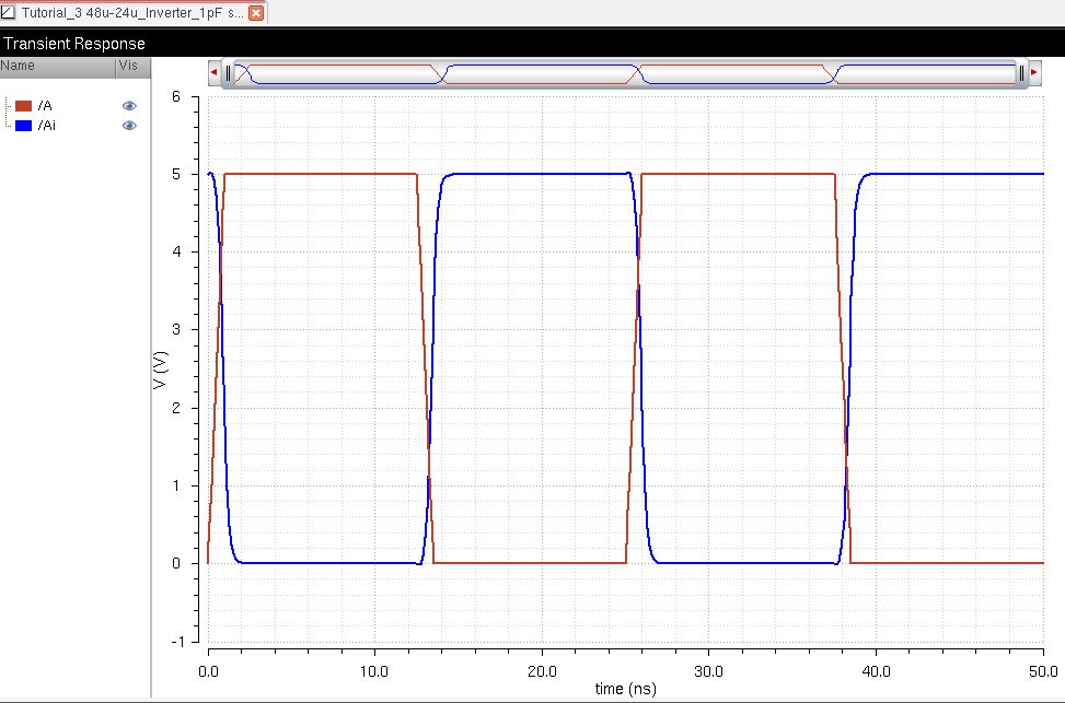 | 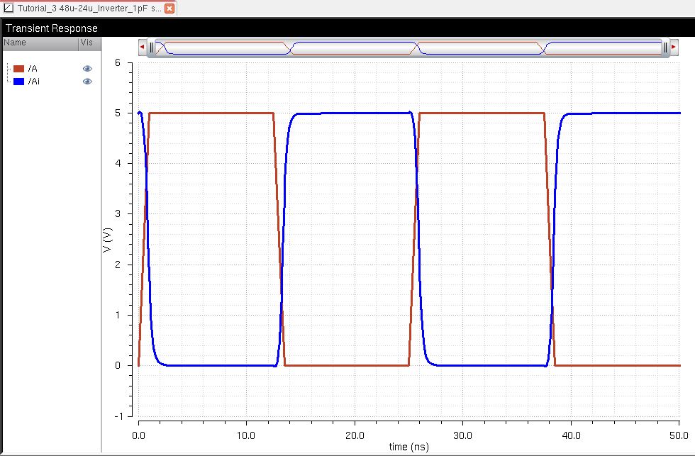 |
| 10pF | 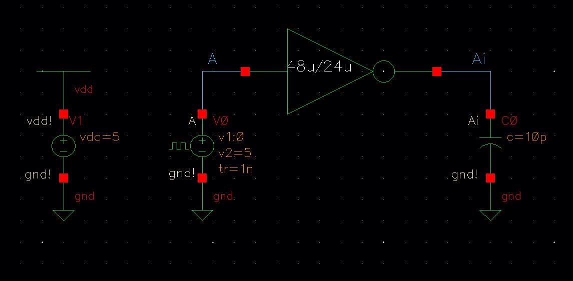 | 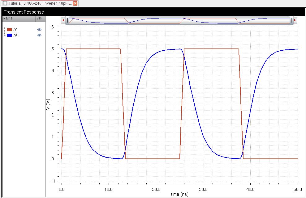 | 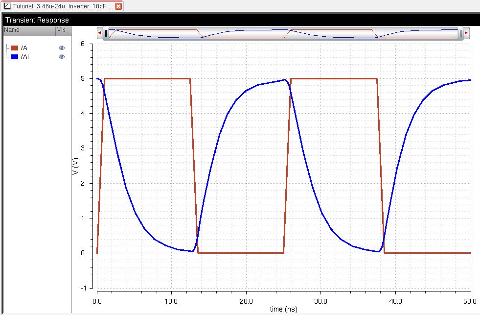 |
| 100pF | 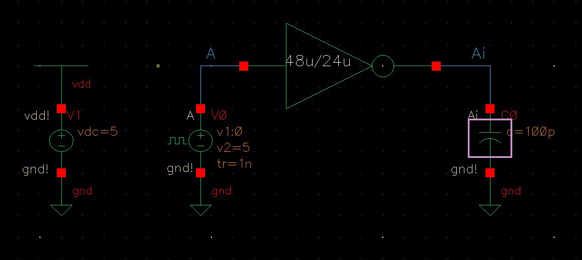 | 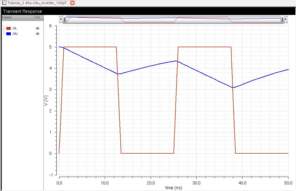 | 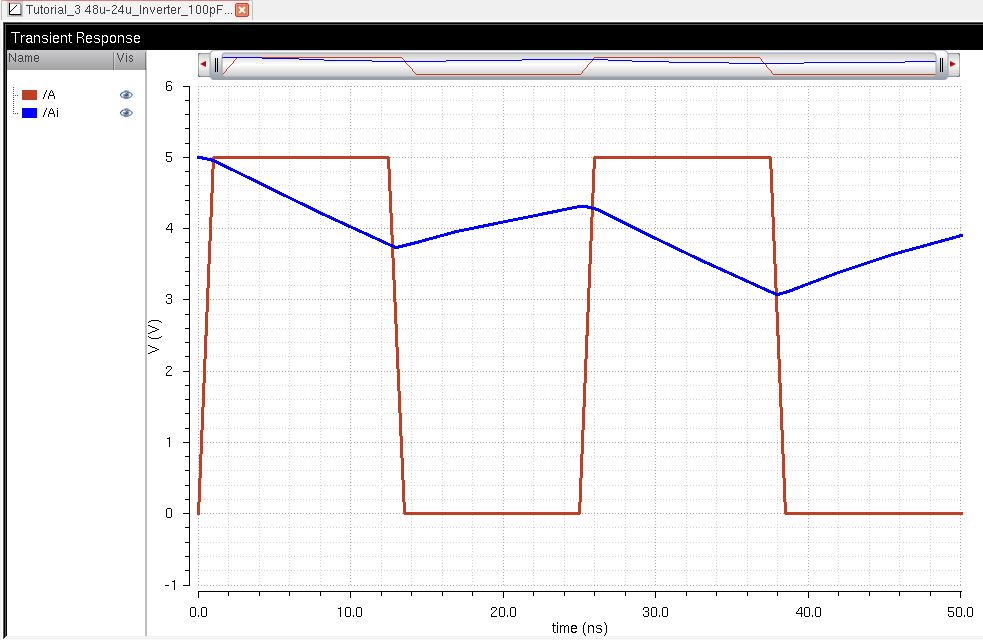 |
| 100fF | 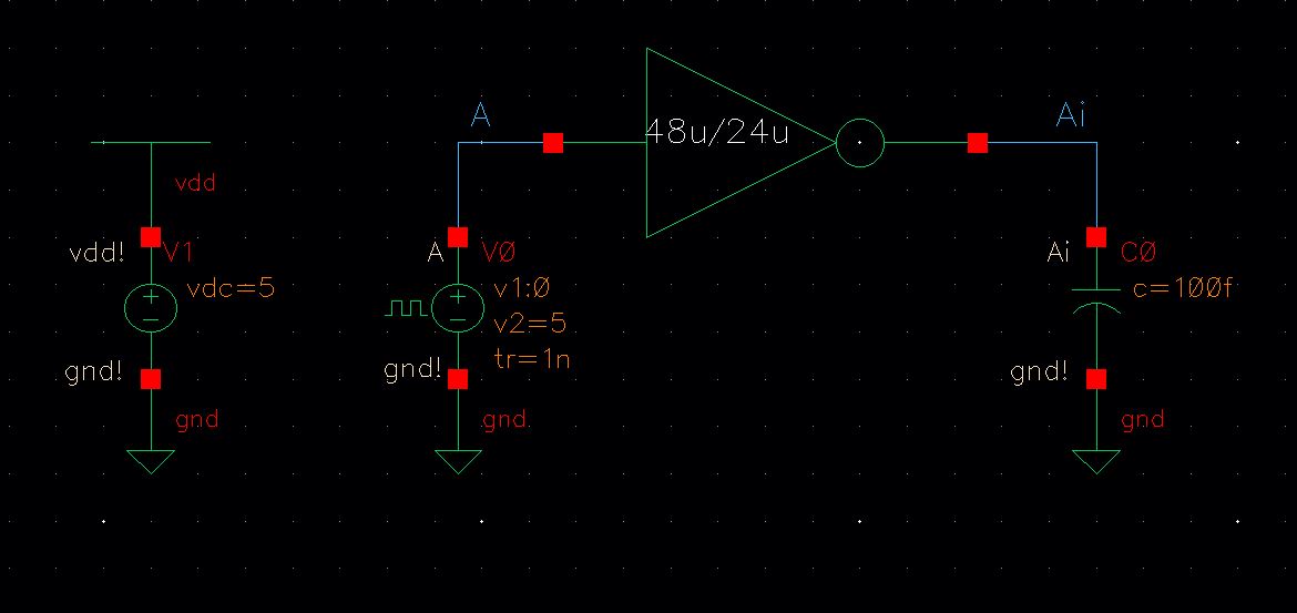 | 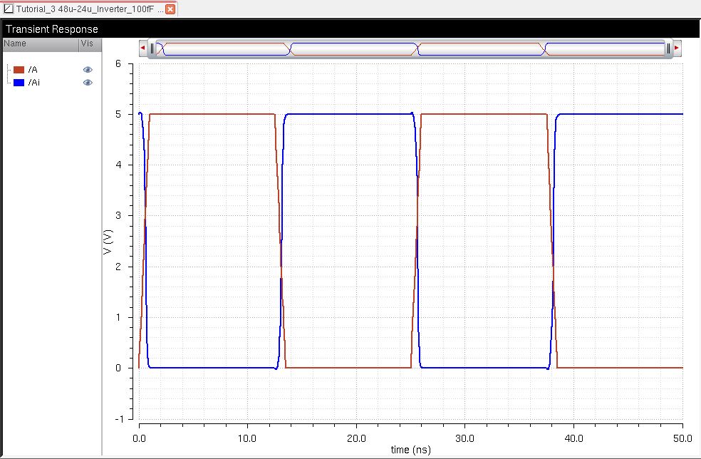 | 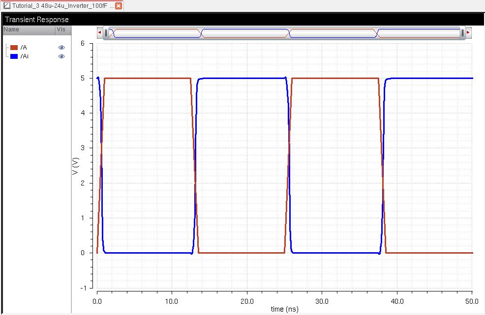 |
Return to Miguel's Labs
Return to EE 421L Labs