Lab 4 - EE 421L
The lab and Tutorial_2 has been read through before starting the lab. While working on the lab it is kept in mind that the body of all NMOS devices (the substrate) should be at ground (gnd!) and the body of all PMOS devices (the n-well) should be at a vdd! of 5V.
We will be learning and experimenting with IV
characteristics and layouts of NMOS and PMOS devices in ON's C5 process.
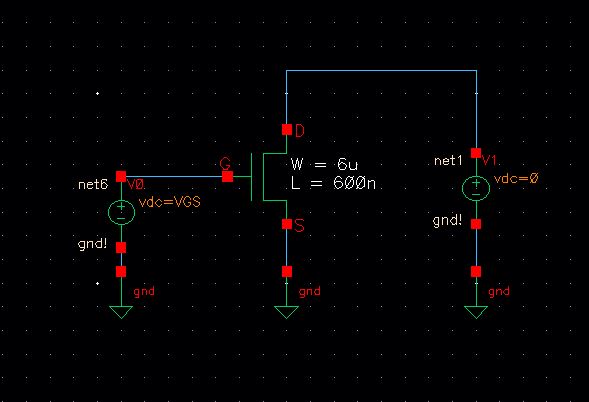
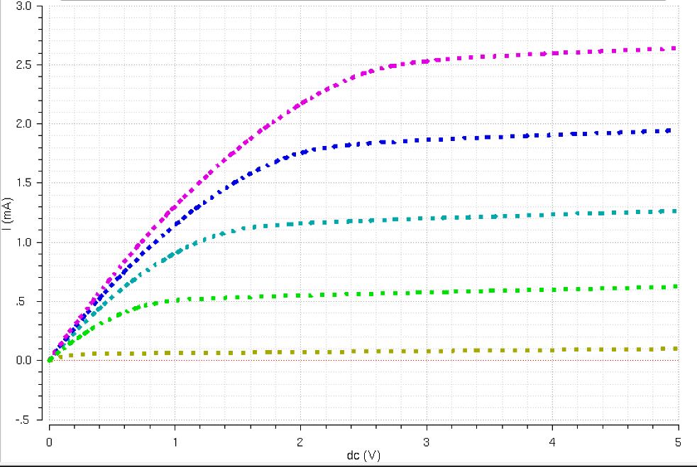
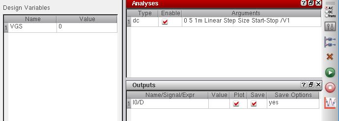
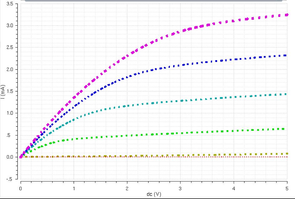
ID v. VDS of an NMOS device for VGS varying from 0 to 5 V in 1 V
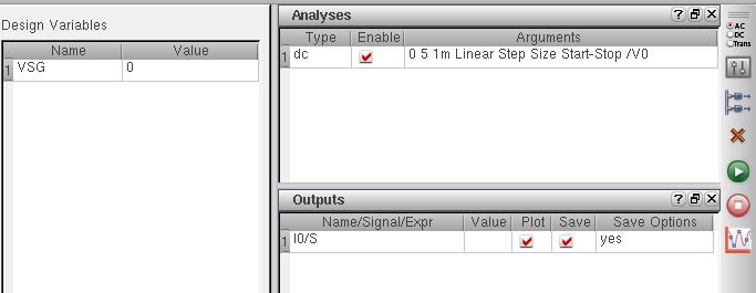
steps while VDS varies from 0 to 5 V in 1 mV steps. It was needed to adjust the
parameter analysis accordingly to change the VGS and VDS values as step
voltages. The simulation yields six results from the step voltages.
  |
 |
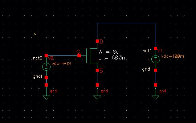
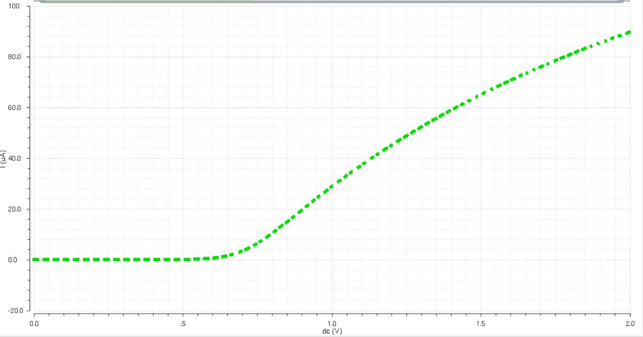
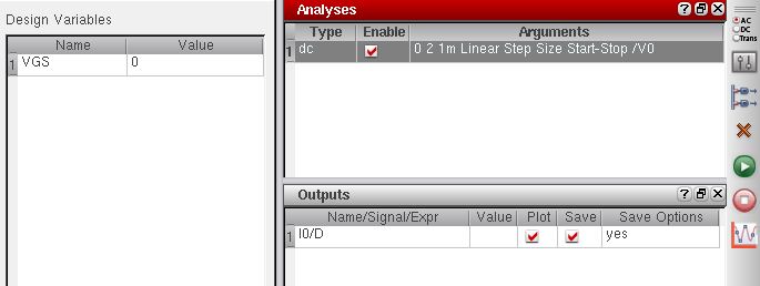
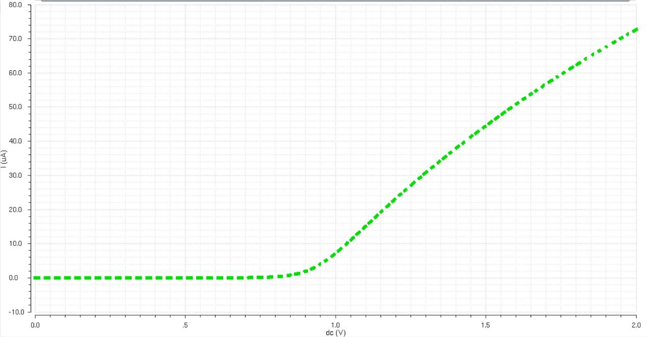
ID v. VGS of an
NMOS device for VDS = 100 mV where VGS varies from 0 to 2 V in 1 mV steps. This
time instead of VDS being 0 and having step voltages it was changed to 100mV
and remained constant with only VGS changing. The parameters were also changed
to get the appropriate sweep.
  |
 |
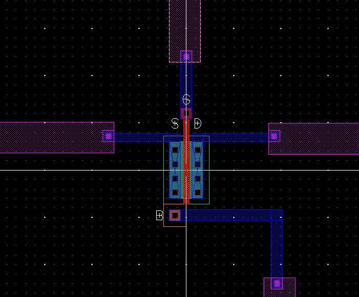
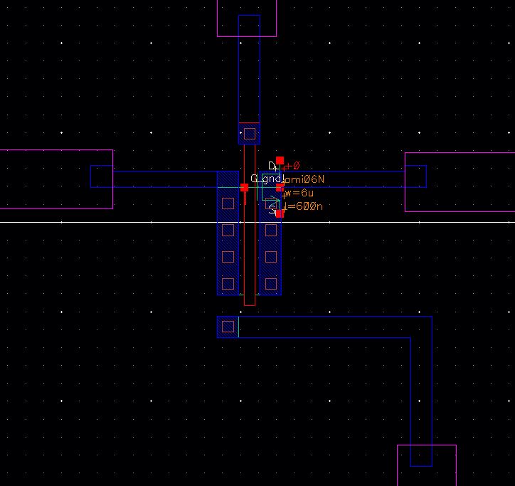
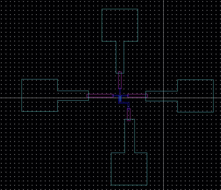
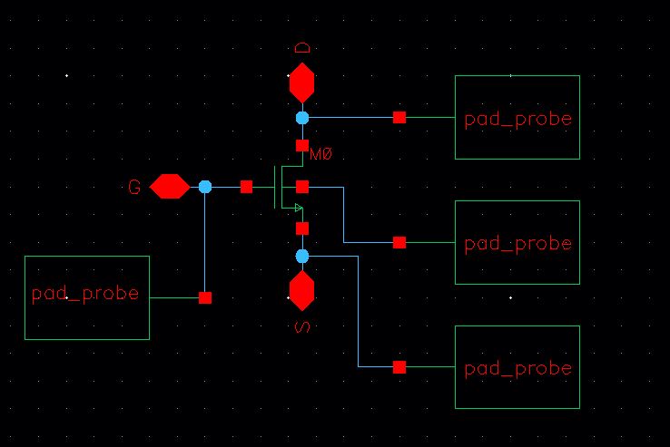
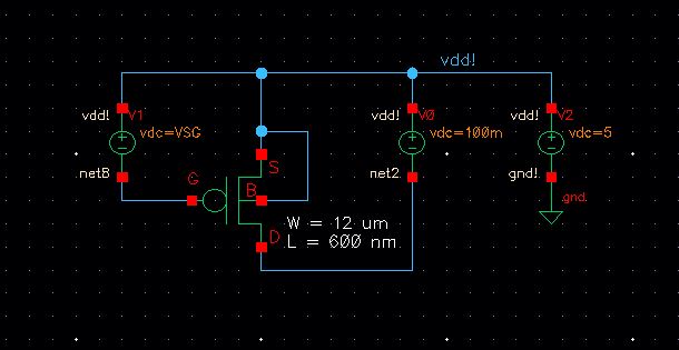
I started by using an NMOS that I previously designed after
watching the Tutorial_2 video. In order to connect the NMOS to the probe pads,
quite a few steps needed to be done. Metal1 connecting from the NMOS had to be
connected to Metal2 but only by using Via1 to connect them. In order to connect
Metal2 to Metal3, Via2 had to be connected in between. This finally allowed
Metal3 to be connected to the probe pad.
 | 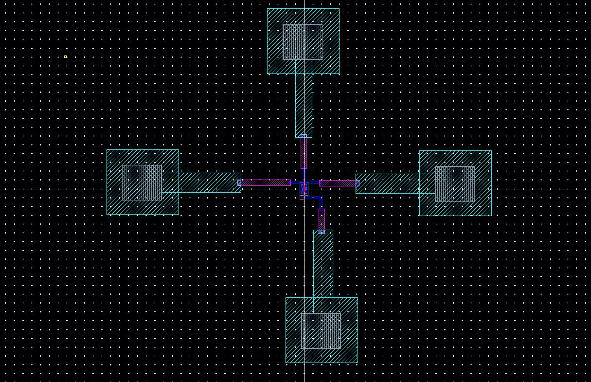 |
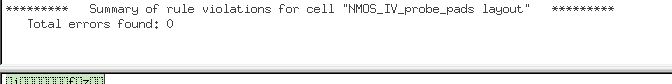
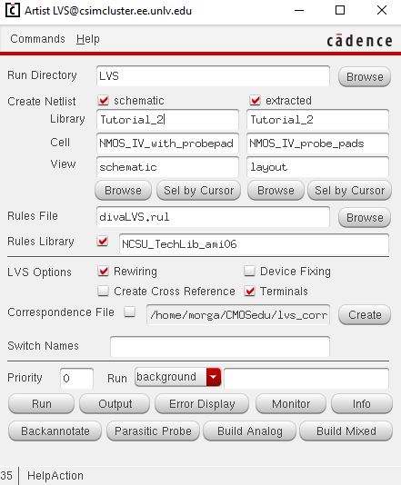
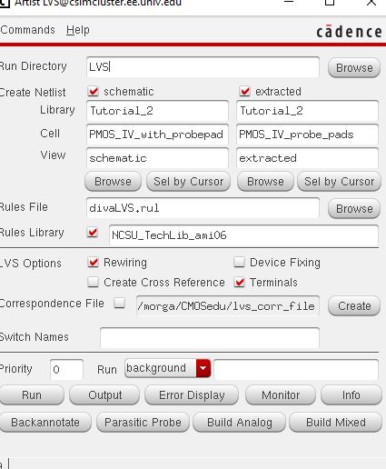
Once I was ready to extract my NMOS file I DRC'd it to make
sure it was free of errors.
 |
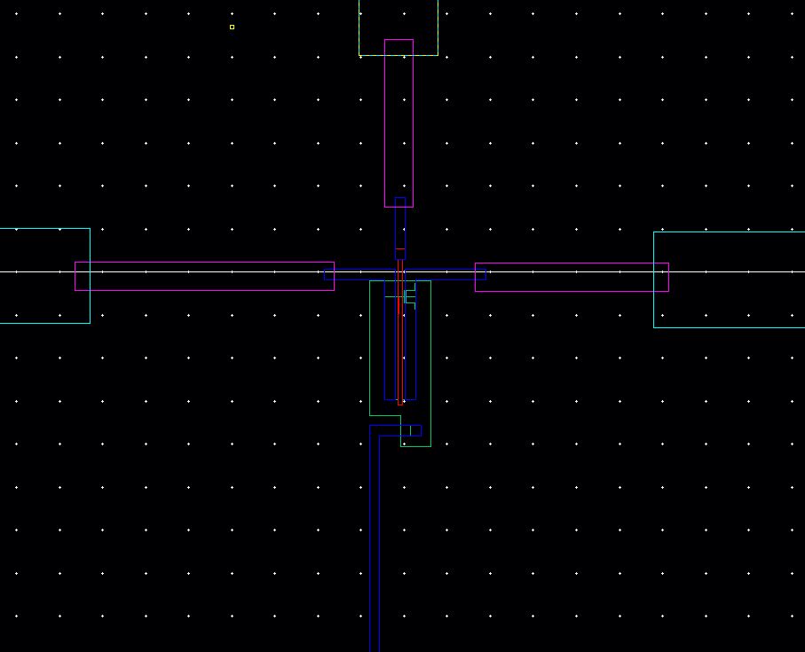
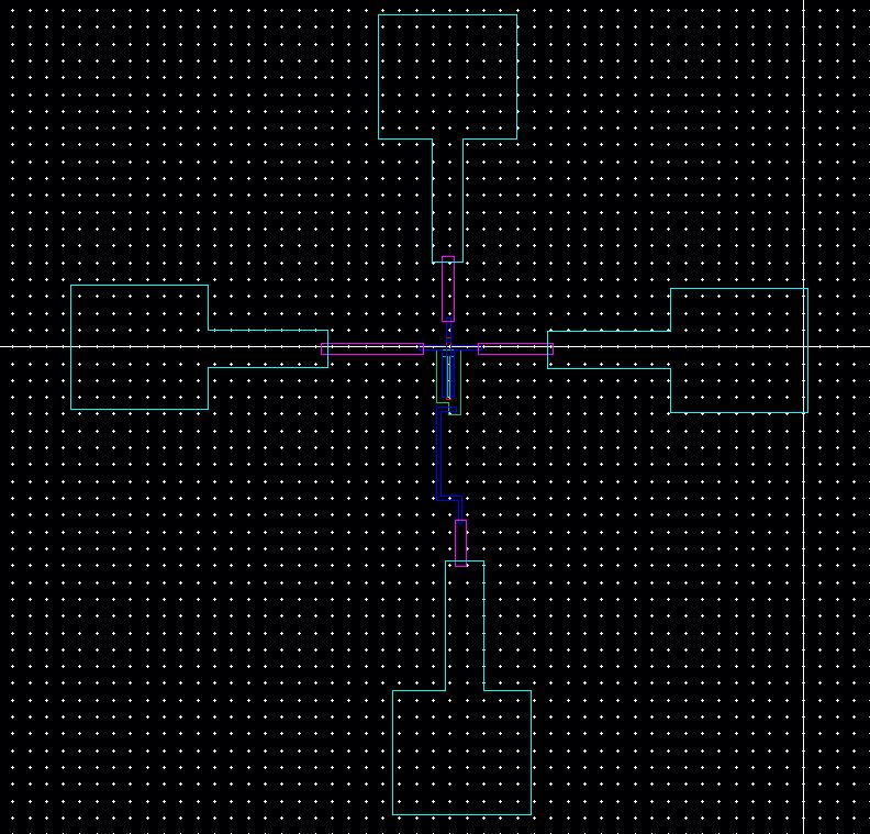
Below are the extracted files of my NMOS design so they can prepare
to be LVS'd. They are images of a close up extraction and a full extraction.
 |  |
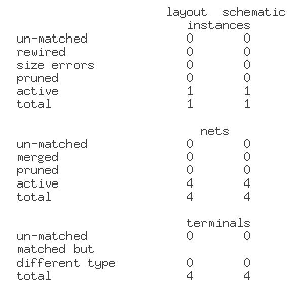
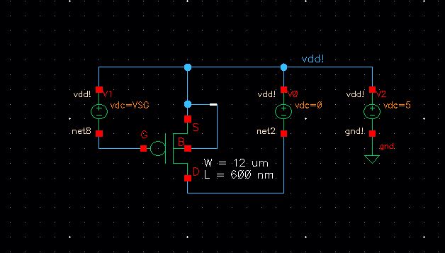
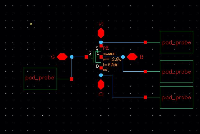
Below is the corresponding schematic so that the layout was
able to be LVS'd properly.
 |  |  |
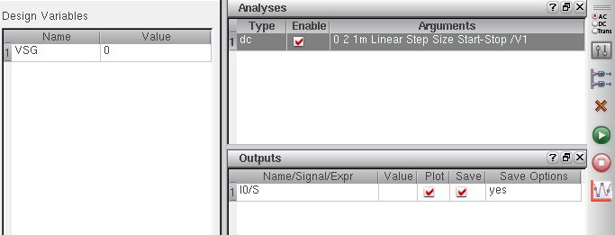
ID v. VSD (note
VSD not VDS) of a PMOS device for VSG (not VGS) varying from 0 to 5 V in 1 V
steps while VSD varies from 0 to 5 V in 1 mV steps. It was needed to
adjust the parameter analysis accordingly to change the VSG and VDS values as
step voltages. The simulation yields six results from the step voltages.
  |
 |
ID v. VSG of a
PMOS device for VDS = 100 mV where VSG varies from 0 to 2 V in 1 mV steps. This
time instead of VDS being 0 and having step voltages it was changed to 100mV
and remained constant with only VSG changing. The parameters were also changed
to get the appropriate sweep.
  |
 |
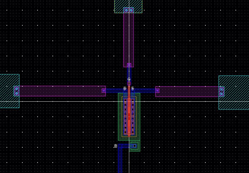
I started by using a PMOS that I previously designed after
watching the Tutorial_2 video. In order to connect the PMOS to the probe pads,
quite a few steps needed to be done. Metal1 connecting from the NMOS had to be
connected to Metal2 but only by using Via1 to connect them. In order to connect
Metal2 to Metal3, Via2 had to be connected in between. This finally allowed
Metal3 to be connected to the probe pad.
 |  |
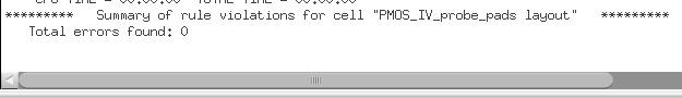
Once I was ready
to extract my PMOS file I DRC'd it to make sure it was free of errors.
 |
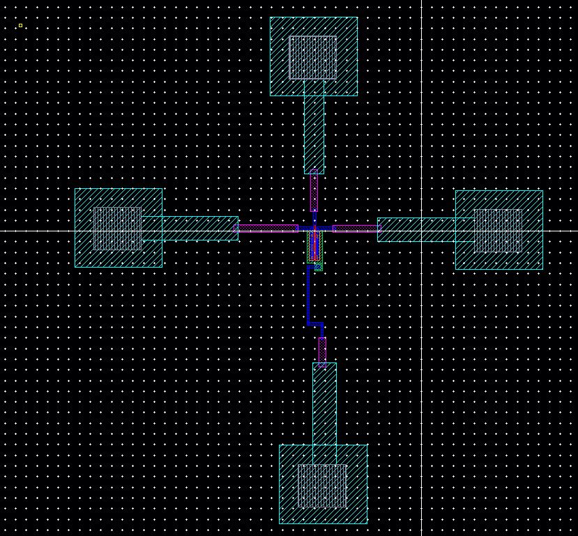
Below are the extracted files of my PMOS design so they can prepare
to be LVS'd. They are images of a close up extraction and a full extraction.
 |  |
Below is the corresponding schematic so that the layout was
able to be LVS'd properly.
 |  | |
Return to Miguel's Labs
Return to EE 421L Labs