Lab 3 - EE 421L
Authored
by Miguel Morga,
September 17, 2017
morga@unlv.nevada.edu
Prelab:
I backed up all of my previous lab work onto my student
drive and onto my usb drive.
Another part of the prelab was to finish Tutorial 1 in order to be able to
continue with Lab 3. Tutorial 1 discusses how to design an n-well resistor and
explains many helpful tools that are offered in the MOSIS program.
Lab Description:
This lab will focus on the layout of the 10-bit
DAC that I designed and simulated in Lab 2. The only difference is that for
this lab I designed it using n-well resistors and explaining the process on how
I made it. Also towards the end of my report, the comparison between my lab 2
schematic and lab 3 layout is made to show that the two are basically
equivalent to one another.
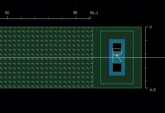
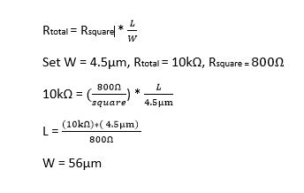
To begin the layout of the resistor I had to figure out the length
and width of it first. I wanted my n-well resistance to be 10k ohms just
like in the previous lab. We know for MOSIS the sheet resistance is
800ohms/square and I just set the width to be 4.5um just like in the tutorial,
since we already knew this value works. I plugged in all these values into the
equation below to find out the length which came out to be roughly 56um.
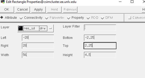
To plug all these values in MOSIS I clicked Q on the n-well part of the
resistor and a window pops up allowing us to change the dimensions. I changed
the dimensions to set the length equal to 56um and the width equal to 4.5um.
The same was done to the n-tap part of the resistor but just to make sure the
width was equal to 4.5um.
The image below shows the equations and the toolbar used to find and edit the
dimensions of the n-well resistors.
 |  |
To make sure the dimensions of the n-well are what I specified it to be all we
have to do is click on the ruler tool. This can either be done by tapping on
the letter k on the keyboard or by going to Tools >> Create Ruler.
The image below shows my resistor being measured by the ruler.
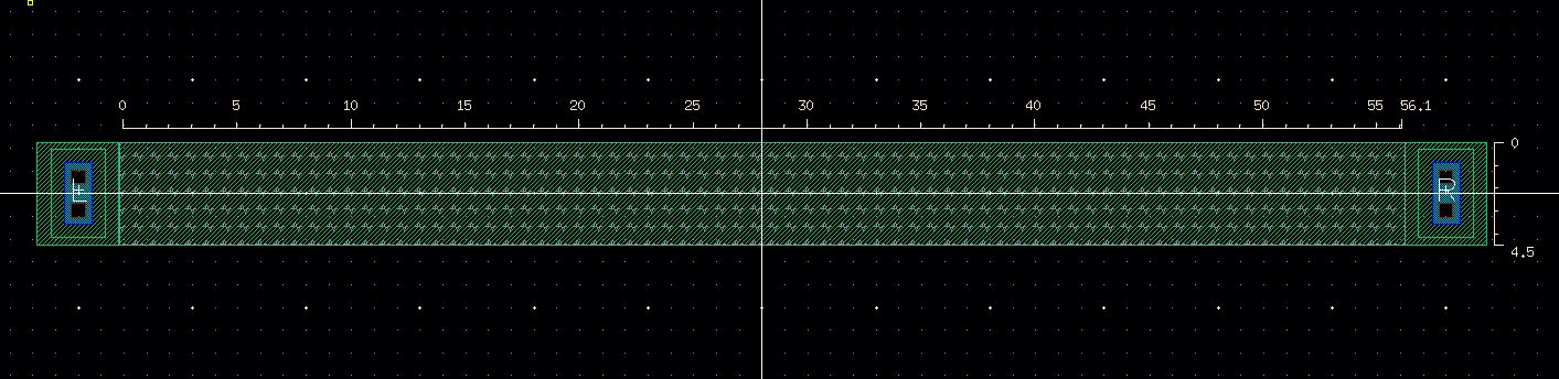
The
image below is the extracted version of my single n-well resistor. I will begin
stacking these to make my DAC now that my resistance value of each resistor is
roughly 10k ohms. It is a little off due to little factors that have to do with
the MOSIS program, but it is the same resistor value as lab 2, so it works.
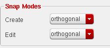
To ensure that each resistor in the DAC is laid out in parallel having the same
x-position but varying y-positions I had to configure the settings a bit. This doesn’t
have to be done but it makes life a lot easier. I went to the top of the
toolbar, followed by selecting Options >> Display >> Snap Modes
>> Choose orthogonal on the create and edit sections. This allows
components in the program to only move in the x or y directions at a single
time. This makes it really easy to stack resistors because you don’t have to
worry about it getting misaligned.
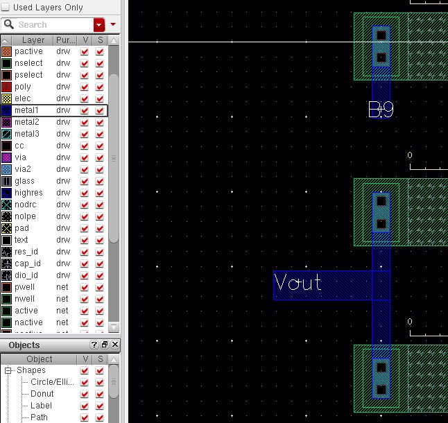
I made sure that all input and output pins were on Metal 1.
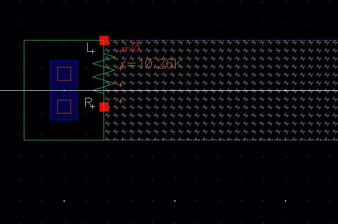
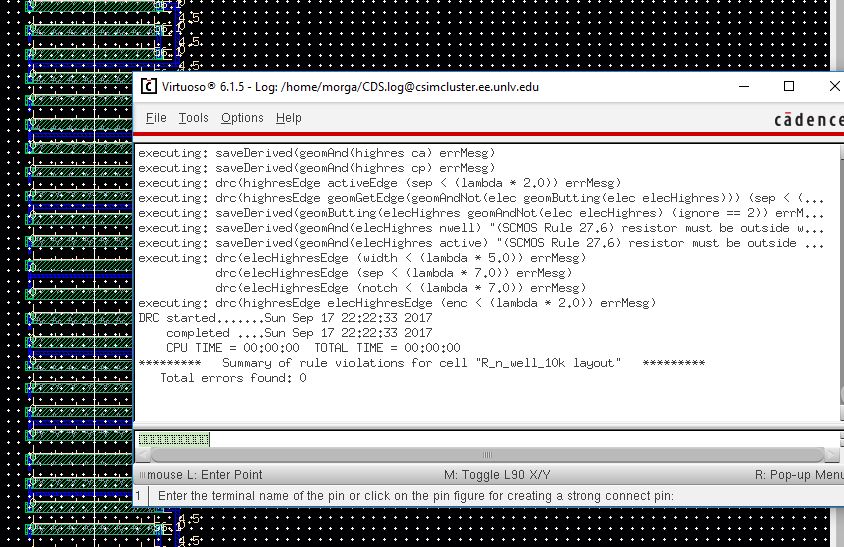
To
examine the results of my DAC I first DRC'd it making sure it was free of
errors which also gets it prepared for extraction. To do this I went to the
toolbar and selected Verify >> DRC.
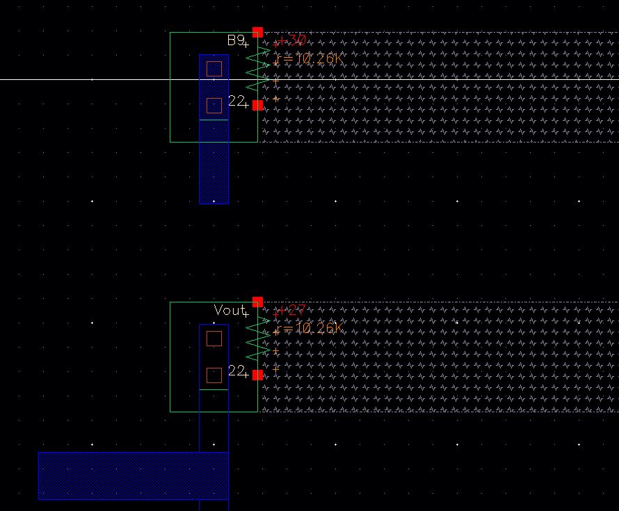
The images below (The left is my design being DRC'd with no errors and the
right is my design after being extracted) are my results. It can be seen that each
resistor in my DAC has a resistance value of 10.26k ohms which means the DAC layout
is accurate.
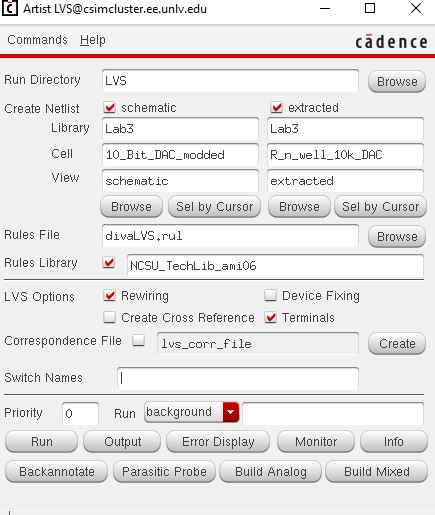
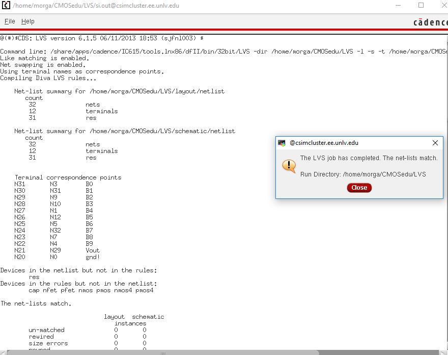
In order to see just how accurate my layout from lab 3 is, I compared it to the
schematic from lab 2. This can be done by a function called LVS (layout vs
schematic). To compare the two, I went to the toolbar followed by Verify
>> LVS. The images below on the left shows what I inputted into the LVS
so that the two designs could be compared. The image below on the right shows
the comparison results from the two designs which shows the two designs are
equivalent.
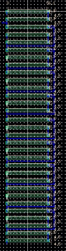
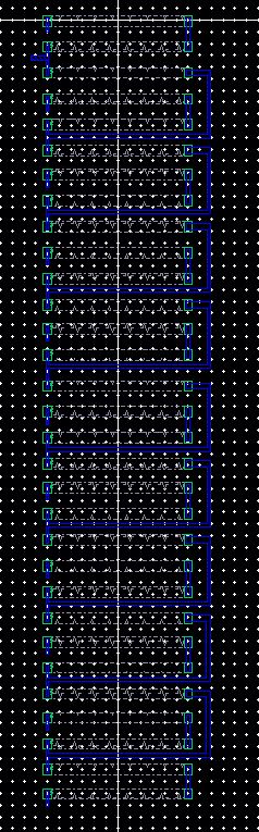
Below are what the final designs of my 10-bit DAC made from n-well resistors look like before and after it was extracted.
Link To Lab 3 Directory
Return to Miguel's Labs
Return to EE 421L Labs